Detector Electronics: Difference between revisions
No edit summary |
|||
| Line 455: | Line 455: | ||
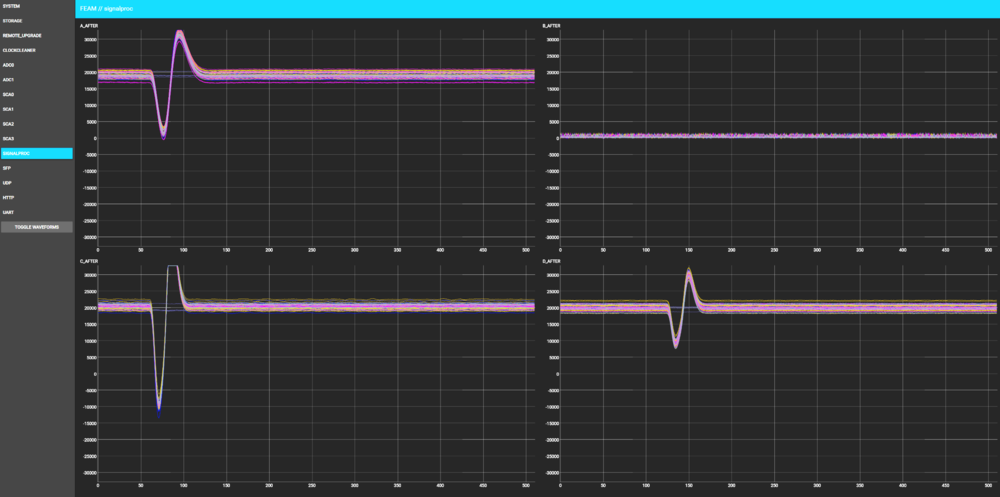
The system monitoring is based on the ESPER protocol provided by the Electronics Development group at TRIUMF. Featuring a built-in web server, with real-time digitizer display, remote upgrade, and JSON-accessible parameters. ESPER allows for real-time diagnostics and testing to be performed on the various electronic modules using either JSON-based requests or a built-in webpage. | The system monitoring is based on the ESPER protocol provided by the Electronics Development group at TRIUMF. Featuring a built-in web server, with real-time digitizer display, remote upgrade, and JSON-accessible parameters. ESPER allows for real-time diagnostics and testing to be performed on the various electronic modules using either JSON-based requests or a built-in webpage. | ||
[[File:image28daq.png| | [[File:image28daq.png|1000x500px]] | ||
<span id="_Toc478997964" class="anchor"><span id="_Toc493676288" class="anchor"></span></span>Figure 23 - ESPER Web Display. Test pulse recorded by the FEAM cards. Individual AFTER chip configuration is visible (gain change, delay). | <span id="_Toc478997964" class="anchor"><span id="_Toc493676288" class="anchor"></span></span>Figure 23 - ESPER Web Display. Test pulse recorded by the FEAM cards. Individual AFTER chip configuration is visible (gain change, delay). | ||
Revision as of 21:06, 19 November 2017
Back to Documentation
Table of Figures
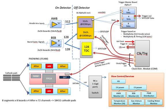
Figure 1 - Overall Data Acquisition scheme 7
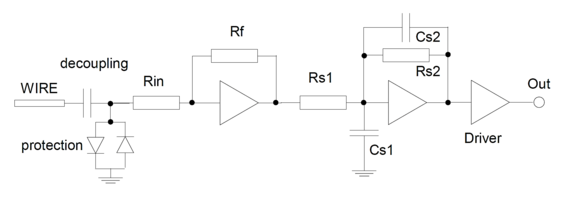
Figure 2 - Anode wire pre-amplification block diagram 8
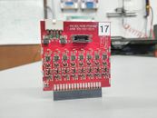
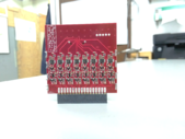
Figure 3 - Anode Wire Board (AWB), 16 channels pre-amplifier 9
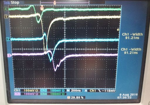
Figure 4 - 4 consecutive anode wire signals 9
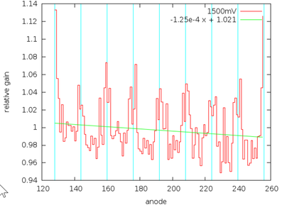
Figure 5 - Anode wire pre-amp gain map for half the chamber circumference 10
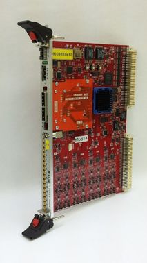
Figure 6 - Alpha16 Data Acquisition Board 12
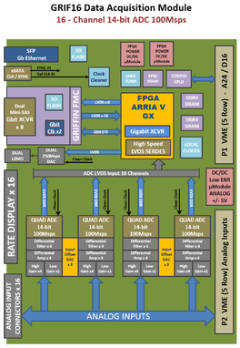
Figure 7 - Grif16 Acquisition Module Block Diagram on which the Alpha-16 is based 12
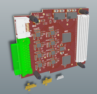
Figure 8 - Model of the new 32channels 12bit @ 65Msps FMC produced in 2016. 13
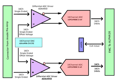
Figure 9 - FMC Alpha-ADC32 Block Diagram 13
Figure 12 - Block diagram of AFTER amplifier 17
Figure 13 - 4 x 72 cathode pad signals, overall time width corresponds to the drift time 17
Figure 14 - Block diagram of one channel of SiPM amplifier 18
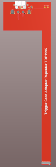
Figure 15 - Trigger Card Adapter and Trigger Card 19
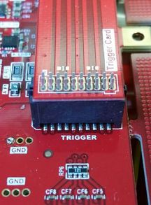
Figure 16 Trigger Card to FEAM 19
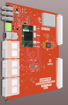
Figure 17 - Clock Distribution Module 20
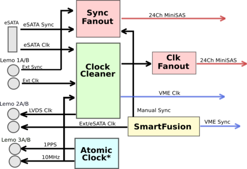
Figure 18 - IO Block Diagram 21
Figure 19 - ALPHA-16 and CDM board in front with the Trigger/Clock distribution cables 22
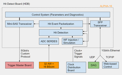
Figure 20 - Hit Detector for the Anode wire and scintillators in ALPHA-16 24
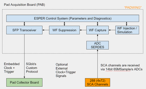
Figure 21 - AFTER chip WFD on the PADWINGS 25
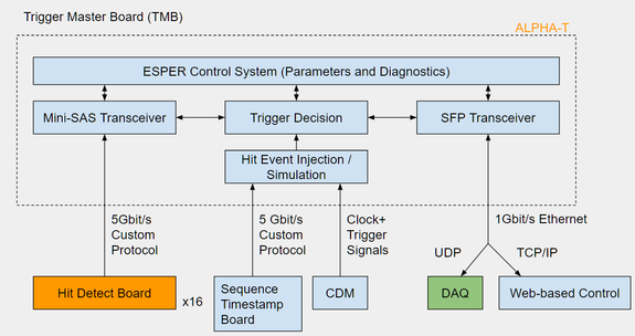
Figure 22 - Trigger decision on ALPHA-T 26
Introduction
This design note describes the electronics chain and components for the readout of the ALPHA-g TPC and barrel scintillator bars.
Scope
The Detector Electronics is composed of 3 independent signal sources:
- Anode Wire signals path
- Cathode Pad signals path
- Barrel Scintillator signals path.
All 3 sources provide a similar function such as signal amplification and conditioning (shaping).
Definitions and Abbreviations
General acronyms or terms used for the ALPHA-g experiment
| TPC | Radial Time projection Chamber |
|---|---|
| Pads | PCB surface seeing the induced anode wire signal |
| SiPM | Si photomultipliers used to detect scintillation light |
| ADC | Analog to digital converter |
| ASIC | Application specific integrated circuit |
| SCA | Switch Capacitor Array ( A type of Waveform Digitizer) |
| TDC | Time to digital converter |
| BSM | Barrel Scintillator Module (64 bars sub-assembly) |
| FEAM, Padwing | Cathode strip acquisition board |
| CDM | Clock Distribution Module |
| BSB | Barrel Scintillator Board |
| WFD | Waveform Digitizer |
Table 1 – ALPHA-g Abbreviations
- AFTER manual
- SensL SPM data sheet
- Edev-group.triumf.ca: contains the FW information on all the Alpha-g custom cards (https://edev-group.triumf.ca/fw/exp/alphag)
Overall Detector Signal Path
The Alpha-g detector provides 3 analog signals that are collected for the track reconstruction to help on the annihilation location in the trap.
- The anode wire signal providing the drift time of the electron through the detector for an angular position.
- The cathode pad signal, which are in-time correlated to the anode wire signal, providing the amplitude of these signals from which the longitudinal position (Z) can be extracted.
- The Barrel Scintillator bar signals provide the time and amplitude of the particle crossing the detector. The Barrel Scintillator is mainly to reject cosmic events. For that purpose, the timing resolution is important. Therefore the BSM analog signal is split early in the chain to record the amplitude and time separately.
The anode wires and the barrel scintillator bars are read out from both ends to provide a coarse Z-position as well. The Data acquisition is therefore made for reading 2x256 anode wire channels, 2x64 barrel scintillator bars and 18432 channels of cathode pads covering the outer detector cylinder.
Figure 1 - Overall Data Acquisition scheme
Anode wire signal path
The design for the anode wires pre-amplifier is based on work done for several other projects used at TRIUMF and other labs.
Each of the 256 anode wires are read-out from two ends. The signals are used to (1) determine phi-position of ionization track; (2) reconstruct its z-position by weighting signals from two wire ends; (3) generate trigger signal. The pre-amplifiers convert the induced current to voltage that is digitized and processed in the readout system. The main requirements for the amplifier circuit are:
- Input impedance must be low enough so detected charge is sensitive to position of event along wire;
- The shape of signal is optimized for sampling frequency (16 ns) and for fast trigger timing (few ns accuracy);
- Linearity range adjusted for ADC used;
- Gain is adjusted for gas amplification of 105
- Amplifier noise is low enough to detect single-electron cluster.
Figure 2 - Anode wire pre-amplification block diagram
Anode wires are HV-decoupled before connected to the amplifier, but additional (not HV) decoupling is needed at amplifier input to accommodate non-zero potential of the input stage. Protection of the amplifier input is using a standard bi-diode configuration. The first stage is a current-sensitive loop with input impedance defined by resistor Rin and trans-impedance (gain) by feedback resistor Rf. The second stage is 2-pole shaper with shaping time constant defined by components Rs and Cs. The last stage is a cable driver.
Overall gain, transfer function and input impedance of the circuit can be adjusted by changing passive components. This adjustment will be done with studying the TPC prototypes.
Amplifiers are deployed on 16-channel cards, 16 boards serve each end of TPC. They are powered by standard +5V and -5V linear supplies. Each card has a test input that is used to measure amplifiers response and to check for malfunction.
Figure 3 - Anode Wire Board (AWB), 16 channels pre-amplifier
The AWB schematic allows for bipolar signal input. This has the advantage to reproduce the full anode wire signal development including the inverted induced pulse from neighbouring wires as seen Figure 4.
Figure 4 - 4 consecutive anode wire signals
The anode pre-amps have an individual test pulse input to provide a quick functional test. It can also be used for calibration purpose. Several tests have been done in this regard, but the overall chain gain is dependent on many variables (chamber geometry, environmental condition (Gas mixture, T, P), pre-amp (layout, components)). Another more common test pulse injection is available by pulsing all the field wires at once (at the boundary of the drift and multiplication region). This technique has the advantage to produce an induced signal on all the anode wires and cathode pads together at the “same” time. Figure 5 shows the gain variation by wire seen when pulsed through the field wire. 2 interesting features are visible:
a) An overall negative slope, indicated by the linear fit. This slope is explained by the pulse attenuation through the field wires distribution.
b) A clear increase in gain for the wires near the anode wire card boundaries, indicated by the cyan lines is not yet well understood. A further test is planned.
Figure 5 - Anode wire pre-amp gain map for half the chamber circumference
Anode Wire Waveform digitizer (Alpha-16)
The output of the AWB is presented to the Alpha-16 waveform digitizer sampling the analog signal at 62.5Msps.
Note: At the time of this report, the WFD 62.5Msps is not yet available. We use the WFD at 100Msps to perform the tests. The firmware is similar to the 62.5Msps and the final test will be reproduced later.
This module provides 16 channels 14bit ADC @100Msps for 50Ohms single-ended analog signal for the barrel scintillator. It also supports a dedicated mezzanine card (FMC) handling 32 channels 12bit ADC @ 65Msps for single-ended 50Ohms analog signals for the Anode wires.
The Alpha-16 board outputs (16ch.@100Msps and 32ch.@62.5Msps) are collected on the main carrier FPGA for transmission through Ethernet to the backend computer.
The board carries multiple I/O connections required for the module configuration, communication, data transfer, signal inputs, see Figure 7.
- Front panel SFP Gbit Ethernet (copper/fiber)
- Front panel eSATA: clock and sync inputs
- Front panel dual LEMO: Diagnostic DAC outputs (250Msps)
- Front panel MCX connector for 16 x ADC inputs
- Rear entry P2 connector for 16 x ADC inputs
- A24/D16 VME interface to MAXV configuration CPLD
- VME configuration flash updates
- VME bridge to FPGA
- FMC custom module connections.
- Dual MiniSAS for Acquisition setup
- 10 x5Gibt Link
- JESD204B Clocks
- Supports 32 Channel ADC LVDS interface
- Amplifier input switches: Front panel MCX connector, Rear Transition Card SMA connector
- Amplifier Gain x1 and x4
- Switch selectable LEMO NIM Input/ DAC outputs
- Micro SD Flash
- DDR3 DRAM – 667MHz – 128M x 23(MT41J128M16HA-15E)
- FPGA - Arria V (5AGXFB3H4F35C4N)
- MAXV CPLD controller (5M2210ZF256C5N) for USB JTAG and VME access
Figure 6. Alpha16 Data Acquisition Board
Figure 7. Grif16 Acquisition Module Block Diagram on which the Alpha-16 is based
FMC – Alpha ADC32
The FMC – ALPHA ADC32 provides single-stage amplification of up to 32 single-ended 50 analog signals, from the Anode Wire Board Pre-Amplifier, to drive two 16 channel 14bit differential, analog to digital converters sampling at 65MSPS. Further, each ADC will provide a 0.9V common mode offset voltage to be fed into the differential driver
A 16 channel 12 bit digital-to-analog (DAC) converter is used to individually apply an appropriate offset voltage to each of the differential amplifier pairs. The Offset voltages span 2.5Vat 1.22mV increments and will output 0V upon power cycle. The DAC is configurable via an SPI interface via the FMC connector.
ADC32 board has the capability to receive and transmit an LVDS clock signal through the eSATA connector which is fed to the FMC connector
Figure 8 - Model of the new 32channels 12bit @ 65Msps FMC produced in 2016.
Figure 9 - FMC Alpha-ADC32 Block Diagram
These notes are for the current revision of the Alpha ADC32, a new revision is currently being talked about
The board is composed of the following elements:
- 400 Pin FMC connector
- Provides SPI interface
- ADC Synchronization
- Support for 32 LVDS analog signals
- Supply voltage of fused +12V, Switched 3.3V and 1.2-3.3V adjustable
- 32 channel Analog inputs via Hirose connector [FX2-40S-1.27DS(71)]
- 1V analog reference voltage [LTC6655BHMS8-3#PBF]
- ±2ppm
- Differential ADC Driver [ADA4950-2YCPZ]
- ±0.2mV Offset
- 9.2nHz / √Hz Output voltage Noise at Gain=1
- Adjustable output common-mode voltage
- Hardware programmable gain of 1x, 2x and 3x
- Dual 16 channel 14bit Analog to Digital converter [AD9249BBCZ-65]
- 2Vp-p input range
- 65MSPS
- ±0.6LSB
- Input Clock of 10-520MHz
- 16 channel 12bit Digital to Analog converter [ADA4950-2YCPZ]
- Programmable offset voltage
- SPI configurable outputs
- Output range ±2.5V, 0V upon reset
- 1.22mV/LSB
- 1 x eSATA Clk-In / Clk-out to and from FMC connector
Cathode pad signal path
The 18432 cathode pads covering the inner surface of the outer wall of the detector are individually connected to a signal acquisition chain. This collected signals will provide the position of the electron avalanche at the anode wire. Combining them in charge, permit the reconstruction of the track passing through the longitudinal direction the detector. While the cathode pads cover a large area (2.7m2), the actual footprint per channel is limited (3.8mmx37.1mm). Therefore a high-density waveform digitizer chain has been chosen based on our previous experience with the T2K experiment, we opted for the AFTER Switched Capacitor Array (SCA) ASIC. The analog signal path is short as the pads themselves are on the backside the physical outer cylinder of the detector and the input signal connectors to the AFTER chips are on the opposite side of the outer cylinder.
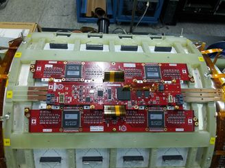
A custom frontend board (FEAM) see Figure 10 handling 288 individual cathode pads has been designed. It is composed of 4 ASIC AFTER (72 channels) with associated waveform digitizer for the individual signal on 512 cells at 20Msps. In addition, an FPGA manages the board services and the data collection and transmission through a 1 gigabit/sec optical link to the Ethernet using the UDP protocol.
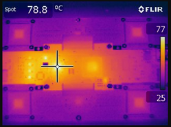
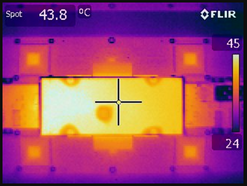
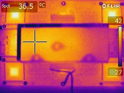
While the power consumption per channel at the ASIC level is low, the power requirement is in the order of 15W per board for a total at the detector level approaching 1000W. This required proper cooling to maintain a reliable operation of the electronics. Figure 11 shows the board temperature with and without cooling plate. Thermal images have been taken to confirm the temperature reduction of the main heat source (Clock cleaner, FPGA, ADC, AFTER in that order). We can guarantee a chip temperature below 60°C to keep the default chip MTBF.
Figure 10 - Cathode Pad Board readout for 288 channels at 62.5Msps, visible 4 AFTER chips, 3 copper bars running under the central board for power distribution
Figure 11 – Thermal image of the FEAM with hot spot temperature: without cooling plate (78°C), with cooling plate (45°C), with cooling plate & water cooling (36°C)
Cathode Pad Circuit
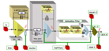
The cathode pads are read-out by AFTER ASIC which diagram is presented in Figure 12. Each channel consists of a charge-sensitive preamplifier, pole-zero cancellation of preamplifier decay time, RC2 shaper and 512-cell SCA to store the waveform. Amplifier gain, pole-zero time constant and shaping time are programmable.
|
Figure 12 - Block diagram of AFTER amplifier |
|
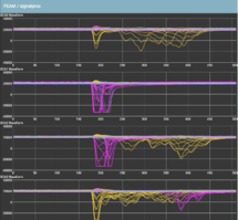
The acquisition of the FEAM cards is operational and initial waveforms can be displayed as seen in Figure 13. This visualization is for monitoring the individual channels only. The data acquisition is using a different path for fast data collection. Figure 13 shows cathode signal examples collected by the FEAM card. The signal shape is consistent with avalanches occurring from a cosmic track going through the detector. The initial pulse corresponds to the early avalanches when the track crosses the amplification region (near the anode wire). The remaining pulses show the later electron avalanches reaching the same anode wire from the drift region due to the track angle. The complex pulse shape from the drift region reflects the convolution in this time base of the arrival of the electron to the amplification region and the induced pulse from the resulting electron avalanche.
Barrel Scintillator signal path
Note: While the Barrel Scintillator is part of the Alpha-g detector for cosmic rejection purpose, this section is still under development. The initial concept and implementation are therefore not final. The volume allocated for it in the other hand well defined due to external to the detector constraints.
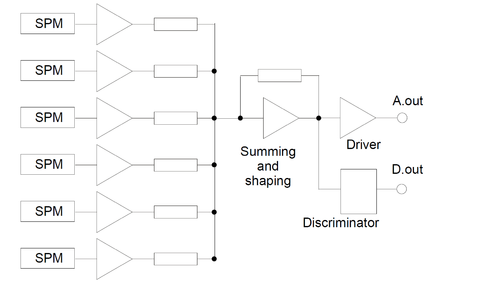
Light at both ends of each bar of the barrel scintillator is collected for a rough position detection of the crossing particle and timing information. To improve the detection information (maximize photon collection), 6 individual SiPM light detector (SensL) are mounted on both ends of the individual scintillator bar for a coverage of 50% of the bar. This assembly is in a light-tight and gas-tight enclosure. A cold gas flows through the box to lower the SiPM temperature operation in order to reduce the dark noise of the device. A shaper/amplifier board (BSB) will be mounted on the outside of the enclosure. Each of the board will acquire the signals of 4 adjacent scintillator bars. In total 64 scintillator bars are read out by 16 boards at each end. A block diagram of one bar readout is shown in Figure 14. The signal gathering of the 6 sensors is based on an analog sum.
Figure 14 - Block diagram of one channel of SiPM amplifier
The 6 pre-amplifier outputs are combined to provide the sum of 6 signals. This resulting signal is further amplified and shaped (if necessary) on a second stage post-amplifier/discriminator. This signal sent to the readout system through a cable driver. Two signals will be acquired from each bar: (1) Analog sum fed to a waveform digitizer with proper digital processing to determine event position and timing; (2) LVDS signal fed to a TDC for off-line precise timing measurement purposes. For the LVDS signal, the post-amplifier will have a controlled threshold voltage to the signal comparator.
The BSB will be powered by standard +5V and -5V linear supplies. Each board has a test input to allow individual board measure of the amplifier response, malfunction test and to provide the necessary services to the light sensors device (Voltage bias, temperature sensor, etc).
The output of the analog output of the BSB will be shaped for the 100Msps WFD and in parallel will issue a digital signal for timing information to a TDC.
Trigger Distribution
On the full-length detector, the FEAM boards will receive trigger and clock signals from the CDM through the Trigger Card Adapter. The adapter receives signals from the CDM via a 7 pin SATA connector. The signals can be re-driven by repeaters on the adapter and are sent down a chain of 7 Trigger Cards with the adapter forming the first link.
While there are other elegant means of distributing the common clock and trigger to all the electronics boards, this method is the most simple and robust.
Figure 15 - Trigger Card Adapter and Trigger Card
Figure 16 Trigger Card to FEAM
A Samtec SFM-110 connects each card to a FEAM board and also provides through holes pins where another card can be overlapped and soldered. In this manner the chain of Trigger Distribution Cards is formed, providing a shared clock and trigger signal to a column of 8 FEAM boards.
Clock Distribution Module
Figure 17 - Clock Distribution Module
- 6x LEMO Connectors [2 Output, 4 Input]
- 6x Mini-SAS providing up to 24 channels of clock and synchronization breakout
- 1x Combination eSATA/USB connector
- eSATA provides CLK and SYNC
- USB provides USB to Serial communication 115200 BAUD
- 1x 10/100 Base-TX Ethernet
- Optional Atomic Clock module support, 10MHz and 1PPS [CSAC - SA.45s]
- Short term Stability <1E-11
- over 1000 seconds (100μHz / 1000s)
- Aging rate of <9E-10 per month (9mHz/month)
- Onboard 10MHz Crystal Oscillator [FOX924B-10.000]
- ±2.5ppm
- ±1ppm per year
- JTAG ARM Support
- SmartFusion2 SoC [MS2-FG484]
- Ultra-low noise clock jitter cleaner 3:15 input to output support [LMK04821]
- Min/Max VCO Frequency 2750/3072MHz
- 0.111RMS Jitter
- TTL and NIM signal compatibility for external CLK and SYNC
- VME - 6U - 3Row
- Approximate Current Draw 1.837A at 5V
The Clock Distribution Module (CDM) has the capability to distribute two externally sourced clock and synchronization signals to six mini-SAS connections for total 24 signal signals. The external signals are provided through the eSATA and LEMO 1A/B Connectors. The module also has the capability to add an Atomic clock that outputs a 10Mhz signal and a 1 Pulse Per Second (PPS), as well as user-defined synchronization signal. Lastly, the module can be configured to output the external clock signals to the LEMO 2B connector or VME bus.
Figure 18 - IO Block Diagram
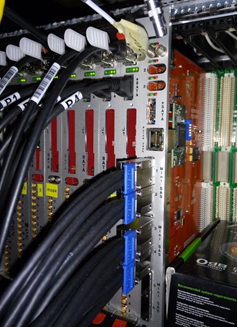
Figure 19 - ALPHA-16 and CDM board in front with the Trigger/Clock distribution cables
Frontend Board Firmware
The firmware (FW) refers to the embedded code running on the Field Programmable Gate Arrays (FPGAs) and microcontrollers (MCUs) located on the various modules within the experiment. These devices store, load, and run the programs required for operation of the different digital electronic components within the experiment.
Firmware code is essential to the operation of the detector as it provides the mechanism to configure the hardware for its particular purpose. Such as analog-to-digital conversion, data filtering, data trigger composition, transport of the data, and orchestration of all the different hardware modules to succeed in acquiring meaningful information across the overall system. Some of the firmware tasks are:
Low-level acquisition of the 3 different WFDigitizers (Anode wire, Cathode pad, Barrel Scintillator)
Links all the electronics boards to the DAQ system.
Collected in real-time information for trigger decision making.
Distribute synchronization signals and trigger to all the acquisition boards.
Provides to the user; configurable board and operation parameters settings.
Provides board monitoring and debugging tools.
Most of the FW code base has been based off of prior code developed for the currently running GRIFFIN experiment, with some exceptions, such as the Trigger Master Module which needed custom code specific to ALPHA-g, and the PADWING, which contained the AFTER SCA chip not present in GRIFFIN.
The firmware code is loaded onto the hardware board where an FPGA or MCU is present. Each firmware module has specific firmware capabilities, detailed as follows:
- Hit Detector firmware Module (ALPHA-16 carrier board)
- Anode Wire and Barrel Scint. signal waveform digitizers acquisition
- Local data filtering for Trigger purpose
- Transmission of summary data to Trigger Module for trigger decision
- Data compression/filtering and retention for transmission to backend on Trigger reception
- Monitoring of hardware functions (U,I,T)
- Configuration of hardware mechanism
- Update of firmware code mechanism
- Pad Acquisition firmware Module (PADWING board)
- Cathode pad signal waveform digitizers acquisition
- Data compression/filtering and retention for transmission to backend on Trigger reception
- Monitoring of hardware functions (U,I,T)
- Configuration of hardware mechanism
- Update of firmware code mechanism
- Master Trigger firmware Module (ALPHA-T board)
- Summary data reception of the multiple GRIF-16 boards
- Trigger decision algorithm
- Packaging of Trigger decision information and transmission to the backend.
- Monitoring of hardware functions (U,I,T)
- Configuration of hardware mechanism
- Update of firmware code mechanism
- Clock and Trigger Distribution firmware Module (CDM board)
- Monitoring of hardware functions (U,I,T,Clock Frequency)
- Configuration of hardware mechanism for clock and trigger distribution
- Update of firmware code mechanism
Hit Detector Module (ALPHA-16)
The Hit Detector firmware module handles the acquisition of the analog input signals from the anode wires and scintillators, the digital conversion of that data, and then the transfer of that data to both the DAQ and the Trigger Master. The first implementation of the hit detection is based on hit multiplicity. Later on, a more sophisticated algorithm will be implemented to determine in real time the timing and charge collected for each channel. This information will be transferred to the Trigger Master for more efficient trigger filtering.
The ADC data is acquired from both the FMC ADC32 ADCs and the onboard 16ch 14-bit ADCs using the FPGAs hardware SERDES modules. These modules de-serialize the data stream from the ADCs into a format suitable for internal analysis for hit detection, and for transfer to the MIDAS DAQ.
Once one or more hits are detected, the ALPHA-16 transmits the hit count to the ALPHA-T for a hit multiplicity test, and then waits for a trigger response to decide to discard or transmit the waveform data associated with the detected hit to the DAQ.
Currently, when a trigger is fired by the Trigger Decision module, all channels transmit their captured waveforms to the DAQ. In the future, only channels that have detected a hit will send waveforms on a trigger.
System monitoring and configuration of the Hit Detector module is handled by ESPER running on a NIOS-II soft-core processor instantiated within the FPGA. The OS used is Micrium µC/OS-II, a small real-time OS licensed by Altera for use with their NIOS-II processor. ESPER performs the remote upgrading of the Hit Detector, viewing of the captured waveforms, and diagnostic reading and writing of all firmware settings and counters via a simple JSON-based interface, or an HTML based webpage.
Figure 20 - Hit Detector for the Anode wire and scintillators in ALPHA-16
Pad Acquisition Module (FEAM)
The pad acquisition firmware module handles the collection of the PAD analog signals captured by the four AFTER ASICs on the module. Capture occurs upon receiving a trigger signal from the Trigger Decision module. Once captured, the AFTER data is transmitted to the MIDAS DAQ over ethernet. No pad information is provided back to the Trigger Decision module.
Each of the AFTER ASICs transmits its captured analog data to a 12-bit ADC which in turn converts the analog signal into digital data and transmits that to the FPGA. The FPGA uses its internal SERDES hardware to de-serialize this data and process it. Once captured, channels that do not contain data of interest are suppressed, and the data is packaged up and sent out over UDP to the MIDAS DAQ.
In the event that the SFP module that provides ethernet connectivity fails, each PAD acquisition module is connected to one other PAD acquisition module via a secondary gigabit link. While currently unused, this link will be used in the future to support a backup link to the DAQ, in the event of a failure of the primary gigabit link.
System monitoring and configuration of the PAD acquisition module is handled by ESPER running on a NIOS-II soft-core processor instantiated within the FPGA. The OS used is Micrium µC/OS-II, a small real-time OS licensed by Altera for use with their NIOS-II processor. ESPER performs the remote upgrading of the Hit Detector, viewing of the captured waveforms, and diagnostic reading and writing of all firmware settings and counters via a simple JSON-based interface, or an HTML based webpage.
Figure 21 - AFTER chip WFD on the PADWINGS
Trigger Master module (ALPHA-T)
The Trigger Master firmware module is to collect information from the anode wires and scintillators to make a real-time decision if the current physics event is to be recorded. That decision is fed to all the readout boards to trigger the storage of this particular event.
Initial trigger decision will be based on hit multiplicity of each of the ALPHA-16 boards. As the ALPHA-16 is acquiring the anode wire and the barrel scintillator signals, both of these 2 pieces of equipment will contribute to the trigger decision. Dedicated link from each of the ALPHA-16 (hit detector) to the Trigger module will be gathering the overall information for a final decision. Hardware trigger signal is then sent from the ALPHA-T to the CDM for distribution to all the acquisition modules to initiate the transmission of their data to the backend computer through UDP. The trigger board will compose a summary of the trigger information which will also be transferred to the backend.
The Trigger Master module contains two Mini-SAS FMCs, and one ‘communication’ FMC, that consists of a SATA, an SFP, and a Mini-SAS connector. This configuration of FMCs allows for up to twenty (20) 1G/2.5G/5G links via the Mini-SAS, in addition to a 1 Gbit/sec Ethernet connection via the SFP, and clock+trigger over the SATA.
Figure 22 - Trigger decision on ALPHA-T
System Monitoring and debugging capability
The system monitoring is based on the ESPER protocol provided by the Electronics Development group at TRIUMF. Featuring a built-in web server, with real-time digitizer display, remote upgrade, and JSON-accessible parameters. ESPER allows for real-time diagnostics and testing to be performed on the various electronic modules using either JSON-based requests or a built-in webpage.
Figure 23 - ESPER Web Display. Test pulse recorded by the FEAM cards. Individual AFTER chip configuration is visible (gain change, delay).
Safety and Hazard considerations
There are no safety or hazard issues in FE system. All amplifiers are low-voltage and low-power circuits built with standard electronics components.
