GSI TRB3: Difference between revisions
| Line 131: | Line 131: | ||
<pre> trbflash program 0x<TRB-address-of-FPGA> ./trb3_periph_padiwa_tdc_32_stretch_triggerlogic28-4_20181024.bit | <pre> trbflash program 0x<TRB-address-of-FPGA> ./trb3_periph_padiwa_tdc_32_stretch_triggerlogic28-4_20181024.bit | ||
</pre> | |||
<pre> | <pre> | ||
Revision as of 19:09, 21 January 2020
TRB3 is an FPGA-TDC board made and sold by GSI. It can achieve ~20ps timing resolution
Documentation
File:Trb3docu.pdf local copy of the manual
File:Trb3.pdf local copy of the schematics
Hardware Information
Power
The TRB3 runs off 50V DC power. The TRB3 needs a fan in order to operate. Between the fan and the TRB3 they draw ~0.5A on 50V.
Clock and Trigger
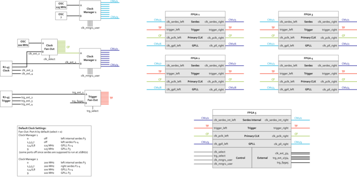
Michael Traxler provided the following picture of clock and trigger circuitry:
Michael also provides following details
Clock:
- system clock frequency of 200MHz can be taken either from the internal oscillator, or via the second LVDS pair (pin 3 and 6) of the connector "RJ-45-Clock". They are distributed to all 5 FPGAs to the primary-clock-input.
- In all "modern" FPGA designs (since several years) you don't have to do anything in registers to use the external clock. The scheme is simple: When an external clock is available and stable and the PLL locks to it at power up, the external clock is used. If not, the internal clock is used.
Trigger:
- If you have a CTS (or a single TRB3 setup) the trigger is generated in the CTS, from external tigger sources. This you can see in Table 27 in the TRB3-manual (currently page 75). For instance, one of the external trigger signals is on pair 2 of the trigger RJ45 connector
- So, for the CTS, there are 4 different inputs available on the two RJ45 connectors, which all can be used at the same time. If you need more, you can add a CTS-AddOn on the backside of the TRB3 and then you have many more trigger inputs. Each input will generate a certain "trigger type" data word in the data stream to distinguish between the trigger inputs.
TDC calibration
The concept of the FPGA-TDC calibration is described here:
http://dabc.gsi.de/doc/dabc2/hadaq_tdc_calibr.html
One important summary from that document: we require ~1e5 random hits for every channel in order to build up an individual fine counter calibration for each channel.
Computer and Software Setup Instructions
Currently have gotten the TRB3 working on three different configurations. On this page we provide information that is generic to each setup. The links provide instructions for the parts of the operation that are unique to each setup:
1) A GSI-provided readout package (and analysis package) which runs on OpenSuse. See TRB3 GSI Opensuse instructions.
2) A MIDAS-based readout on an Opensuse machine. No instructions.
3) A MIDAS-based readout on a Centos-7 machine. See TRB3 Centos-7 instructions.
On this page we provide information that is generic to each setup. The links provide instructions for the parts of the operation that are unique to each setup:
We setup TRB3 on a private network. So need machine with second ethernet port.
Useful TRB3 commands
a) Get IDs for TRB3 FPGAs (1 central FPGA and 4 FPGAs for TDCs):
trb3_user@linux-klyr:~/lindner> trbcmd i 0xffff
0xc001  0xe1000006e937ac28  0x05
0x0100  0x9c000006e937a028  0x00
0x0101  0x91000006e95e8328  0x01
0x0102  0x75000006e9383128  0x02
0x0103  0xe6000006e96e5228  0x03
The four FPGAs that actually make TDCs are numbered 0x100, 0x101, 0x102, 0x103.
b) Print out raw TDCs for the events that are coming in through event builder
hldprint localhost:6789 -onlytdc 0x0100 -num 0
c) Print out raw TDCs for events in file
hldprint //data/trb3_data/pulser17342114715.hld -onlytdc 0x0100 -num 0
d) Print out raw data stream from EB
hldprint localhost:6789 -raw
e) Check the status of the clock
Check bit 8 of register 0xd300.
This indicates that an external clock is being used
[agtdc@daq16 triumf_trb171]$ trbcmd r 0xc001 0xd300
0xc001  0x00000101
This indicates that an internal clock is being used
[agtdc@daq16 triumf_trb171]$ trbcmd r 0xc001 0xd300
0xc001  0x00000001
f) "Ping of death" somehow ping board to reboot it:
ping -pc001 trb171
Updating TRB3 firmware
Based on instructions from Michael
General points:
- Take care that you have a stable setup with the power-supply stable and cooling ok, as if you turn off the board while reprogramming you need a programming cable to recover the FPGA.
- List of available firmware files are here:
https://jspc29.x-matter.uni-frankfurt.de/trbweb/?action=page&url=design-files
Steps to flash
1) Get firmware. Ie:
wget http://jspc29.x-matter.uni-frankfurt.de/bitfiles/trb3_periph_padiwa_tdc_32_stretch_triggerlogic28-4_20181024.bit
2) reflashing is done via:
trbflash program 0x<TRB-address-of-FPGA> ./trb3_periph_padiwa_tdc_32_stretch_triggerlogic28-4_20181024.bit
trbflash program 0x0102 ./trb3_periph_padiwa_tdc_32_stretch_triggerlogic28-4_20181024.bit
trbflash program 0x0103 ./trb3_periph_padiwa_tdc_32_stretch_triggerlogic28-4_20181024.bit
3) after a successful flash and verify (automatic):
trbcmd reload 0x<TRB-address-of-FPGA>
4) But do it one FPGA after the other, if you do it the first time. You can also reprogramm all of them at once with a broadcast address.
