Cathode Pad Electronics: Difference between revisions
No edit summary |
No edit summary |
||
| Line 70: | Line 70: | ||
| 1912 || 4283 || 3213 || 1268 || 1945 | | 1912 || 4283 || 3213 || 1268 || 1945 | ||
|} | |} | ||
=== Reference === | |||
[[File: AFTER_MANUAL_v2.pdf]] | |||
Revision as of 23:15, 4 May 2017
The cathode pads are read-out by AFTER ASIC. One chip has 72 active channels and 4 reference channels for pedestal subtraction. Each channel consists of charge-sensitive preamplifier, pole-zero cancellation of preamplifier decay time, RC2 shaper and 512-cell SCA to store waveform. Amplifier gain, pole-zero time constant and shaping time are programmable. Detailed information is in the manual, but the most relevant slow control settings are summarized in the following tables.
The full range of the AFTER chip and the ADC is ±1V, the gain setting determines what charge that corresponds to, leading to a gain value.
| Gain setting | Charge range (fC) | Gain (mV/fC) |
|---|---|---|
| 0 | 120 | 8.333 |
| 1 | 240 | 4.167 |
| 2 | 360 | 2.778 |
| 3 | 600 | 1.667 |
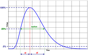
The peaking time is defined as the time the pulse takes to go from 5% to 100% pulse height.
| Time setting | Peaking time (ns) |
|---|---|
| 0 | 116 |
| 1 | 200 |
| 2 | 412 |
| 3 | 505 |
| 4 | 610 |
| 5 | 695 |
| 6 | 912 |
| 7 | 993 |
| 8 | 1054 |
| 9 | 1134 |
| 10 | 1343 |
| 11 | 1421 |
| 12 | 1546 |
| 13 | 1626 |
| 14 | 1834 |
| 15 | 1912 |
This peaking time translates to other relevant times as shown in the next table.
| Peaking time (5%-100%) | Fall time (100%-5%) | FWHM | Rise time (50%-100%) | Fall time (100%-50%) |
|---|---|---|---|---|
| 116.7 | 202.5 | 158.4 | 67.59 | 90.82 |
| 200 | 438.2 | 311.6 | 121.3 | 190.3 |
| 505 | 1194 | 843 | 329.2 | 513.7 |
| 993 | 2351 | 1689 | 656.1 | 1033 |
| 1912 | 4283 | 3213 | 1268 | 1945 |
