VME-ALPHA-TTC: Difference between revisions
Jump to navigation
Jump to search
m (New page: == VME-ALPHA-TTC - ALPHA (CERN AD-5) Si vertex detector control module == === References === * [http://edev.triumf.ca/projects/edevel00023] VME-NIMIO32 (REA 131) project page on edev.tri...) |
mNo edit summary |
||
| Line 11: | Line 11: | ||
=== General characteristics === | === General characteristics === | ||
==== Photos ==== | ### ==== Photos ==== | ||
### | |||
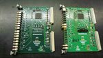
[[Image:VME-NIMIO32-Rev0-Rev1.jpg|150px|Rev0 and Rev 1 boards | ### [[Image:VME-NIMIO32-Rev0-Rev1.jpg|150px|Rev0 and Rev 1 boards]] | ||
==== Available hardware ==== | ==== Available hardware ==== | ||
| Line 92: | Line 89: | ||
* firmware sources [[http://ladd00.triumf.ca/viewvc/daqsvn/trunk/VME-NIMIO32/MAX3000A_Addr_decode]] | * firmware sources [[http://ladd00.triumf.ca/viewvc/daqsvn/trunk/VME-NIMIO32/MAX3000A_Addr_decode]] | ||
* board Rev0 [[http://ladd00.triumf.ca/viewvc/daqsvn/trunk/VME-NIMIO32/MAX3000A_Addr_decode/VME_Addr_decode.pof?revision=37&view=co]] | * board Rev0 [[http://ladd00.triumf.ca/viewvc/daqsvn/trunk/VME-NIMIO32/MAX3000A_Addr_decode/VME_Addr_decode.pof?revision=37&view=co]] | ||
Revision as of 14:49, 17 September 2012
VME-ALPHA-TTC - ALPHA (CERN AD-5) Si vertex detector control module
References
- [1] VME-NIMIO32 (REA 131) project page on edev.triumf.ca
- [2] Rev0 board schematics
- [3] Rev1 board schematics
- [4] Svn repository for VME-NIMIO32 firmware
- [5] Misc documentation
General characteristics
- ==== Photos ====

Available hardware
- Altera cyclone 1 FPGA: EP1C6Q240C6N
- Serial flash for FPGA configuration: Altera EPCS16
- External SDRAM memory
- VME interface: VME-D[31..0] bidirectional, VME-A[19..0] input only, DTACK output, no BERR, no RETRY/RESP. VME-A[31..20] input only connected only to address decoder FPGA (Altera MAX-something CPLD). This permits all single-word transfer modes, 32-bit DMA (BLT32) and 2eVME DMA (only drives D-lines, but still faster than BLT32). 64-bit DMA (MBLT64) and 2eSST are impossible.
- 16 NIM outputs
- 16 NIM inputs
- 16 ECL/LVDS inputs compatible with LeCroy 4616 ECL/NIM/ECL converter. (Except: Rev0 boards have an incompatible ECL connector)
- 16 "red" and 16 "green" LEDs
- 1 "VME access" LED
- 1 RJ-45 high speed serial I/O interface
Firmware functions
Generic IO32 firmware can include a number of functions. Not all functions are available all at the same time due to resource limitations on the FPGA. Refer to VME Registers for detailed information.
- 20 MHz 32-bit timestamp clock register
- 16 bits of NIM output register (first 4 NIM outputs are multi-function)
- 16 bits of NIM and 16 bits of ECL/LVDS input register with latch function.
- 32 scalers 32 bit, 300 MHz counting rate
- 20 MHz 32-bit timestamp clock register
- 4 timestamp registers using the 20 MHz timestamp clock. Any of the 32 inputs can be routed into any of the 4 timestamp registers.
- trigger counter, trigger timestamp functions for NIM_IN[1] and DAQ busy functions for FP_NIMOUTPUT[1].
- 20 MHz clock for VF48 ADC and VT48 TDC
- 40 MHz clock for V1190 TDC.
- example pulse generator (programmable period 32 bit 10 ns, fixed width 100 ns)
- example L222-like delay and gate generators (NIM_IN[2]/NIM_OUT[2])
- experimental 4-channel TDC. 10 ns base clock with 0.3 ns interpolation ladder (1 ns RMS).
Firmware update procedure
- obtain and build the VME programmer (srunner_vme) and IO32 test program (test_VMENIMIO32):
- mkdir $HOME/packages
- cd $HOME/packages
- svn checkout https://ladd00.triumf.ca/svn/daqsvn/trunk/vme (username svn, password svn)
- cd vme
- make -k srunner_vme.exe srunner_vme_gef.exe test_VMENIMIO32.exe test_VMENIMIO32_gef.exe
- read the firmware revision from VME register 0:
- ./test_VMENIMIO32_gef.exe --addr 0x100000 --read 0
- write Cyclone 1 FPGA firmware into the flash memory using the VME programmer:
- ./srunner_vme_gef.exe -program -64 VME-NIMIO32.pof 0x100020
- !!!be careful about using Rev0 pof files for Rev0 boards and Rev1 pof files for Rev1 boards!!!
- reboot the Cyclone 1 FPGA into the new firmware (requires "fpga-reset" mod):
- ./test_VMENIMIO32_gef.exe --addr 0x100000 --reboot
Firmware revisions
Firmware for the main FPGA:
- firmware sources [[6]]
- firmware schematics [[7]]
- pof files for Rev0 [[8]]
- pof files for Rev1 [[9]]
- 0x01100810 - DO NOT USE - first revision of generic firmware
- 0x01100818 - [[10]] - fixed bug in scaler[6], rearranged TSC4 registers.
- 0x01100914 - Rev1 - [[11]] - add NIM output functions: VME AS and DS outputs, example L222 delay generator
- 0x01101018 - Rev1 - [[12]] - add simplified trigger timestamp functions, add 40MHz V1190 clock output, add T2KM11 trigger function
- 0x01101019 - Rev0 - [[13]] - same as 0x01101018
- 0x01101105 - Rev0 - svn rev 109 - fixed problem with long pulses being miscounted by scalers
- 0x01101118 - Rev1 - svn rev 112 - improved S1249 trigger, output V1190 40 MHz clock on NIM_OUT[3]
- 0x01110702 - Rev1 - svn rev 144 - DO NOT USE - updated the VME interface - DO NOT USE - broken UniverseII VME access (V7805, V7750)
- 0x01110811 - Rev1 - svn rev 159 - no changes. fix for UniverseII VME access.
- 0x01110811 - PPG32-Rev1 - svn rev 160 - no changes. fix for UniverseII VME access.
- 0x01120523 - Rev0, Rev1 - svn rev 169 - implement new scalers (old scalers were lossy)
- 0x01120706 - Rev1 - svn rev 187 - NIM input/output 2 provides V1190 TDC trigger signal synchronized with the 40 MHz V1190 clock.
Unless otherwise notes, because of FPGA resource constraints, firmware for Rev0 boards have 16 scalers for NIM_IN[15..0] and have no scalers for ECL/LVDS inputs. Firmware for Rev1 boards has 4 scalers for NIM_IN[3..0] and 16 scalers for ECL/LVDS inputs.
Firmware for the VME address decoder: