DarkLight
DarkLight experiment at TRIUMF
Links
- https://web.accel.triumf.ca/elinac_elog/frames.pl
- https://driverdisplays.dev.kube.dmz.triumf.ca/elinac
- https://daq00.triumf.ca/mhttpd-dl/
- https://daq00.triumf.ca/elog-dl/
- https://dl-server-2/slowctrl/
- https://daq13.triumf.ca - detector facility daq station
- https://daq17.triumf.ca - MOB GEM lab daq station
- DL-DB - trigger detector SiPM board and distribution board documentation
- https://daq00.triumf.ca/AgWiki/index.php/Chronobox - DL-TDC base firmware documentation
- DL-TDC - DL-TDC special documentation
- VME-PPG32 - PPG32 documentation
- VME-NIMIO32#DL_clock_(PPG32) - PPG32 (IO32) firmware documentation
- chronobox_software - DL-TDC MIDAS frontend git repo
Source code
- git clone https://bitbucket.org/expalpha/chronobox_firmware.git - branch dl-tdc - DL-TDC FPGA source code
- git clone https://bitbucket.org/ttriumfdaq/dldb - DLDB midas frontend, web page and test code
- git clone https://bitbucket.org/ttriumfdaq/dlana - online/offline analyzer for DL-TDC data
- git clone dldaq@daq00.triumf.ca:public_html/git/dlana - dlana local copy
- git clone https://bitbucket.org/ttriumfdaq/dlcfmdb - DL-TDC calibrations database
- git clone dldaq@daq00.triumf.ca:public_html/git/dlcfmdb - dbcfmdb local copy
Drawings
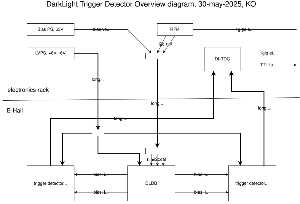
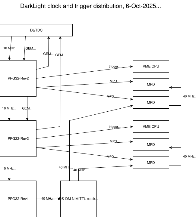
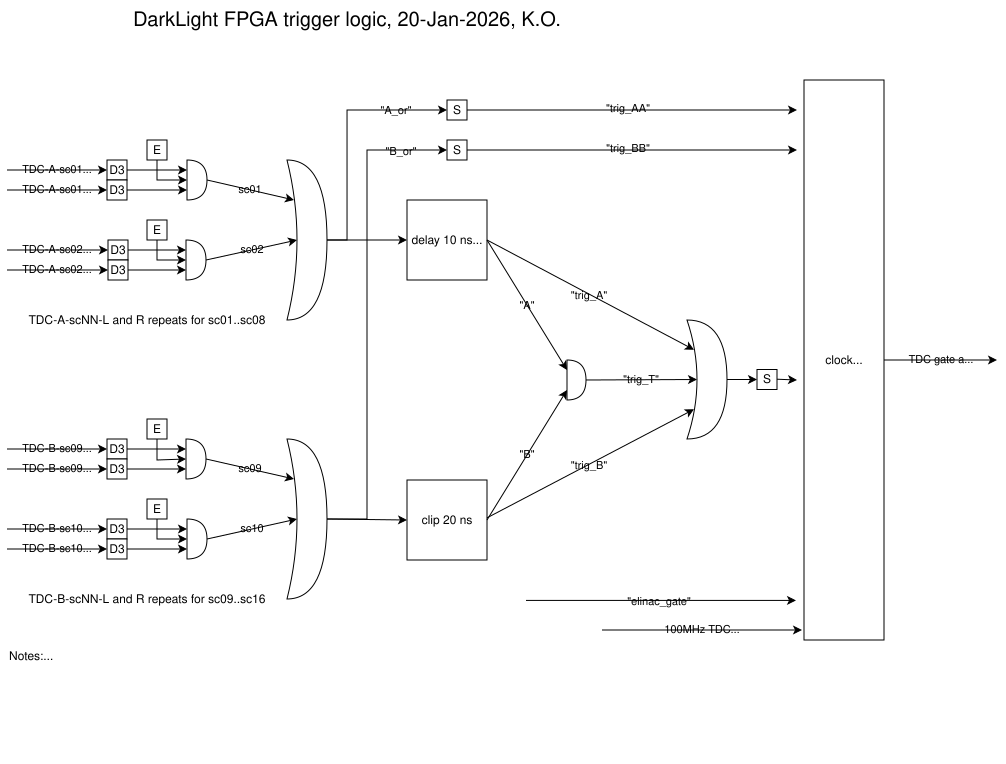
Please click on the SVG-format drawings to see the full image with full text (mediawiki preview truncates the text)
SVG format - trigger detector diagram
SVG format - trigger and clock distribution
SVG format - FPGA trigger logic=
PDF format drawings
- File:DL-trigger-detector.drawio.pdf
- File:DL-trigger-clock.drawio.pdf
- File:DL-trigger-fpga.drawio.pdf
DAQ
- ODB /eq/cb02/settings:
- dl_ctrl for A+B 0xC0FE
- dl_ctrl for A*B 0xC0F0
- A is grand-OR of all scintillators on the TDC-A cable (enabled by dl_trg_mask[7..0], 8 bits for the 8 scintillators)
- B is grand-OR of all scintillators on the TDC-B cable (enabled by dl_trg_mask[15..8], 8 bits for the 8 scintillators)
- each scintillator signal (A[7..0] and B[7..0]) is L*R hardwired in dl/dl.sv
- dl_tdc_mask can be used to disable each of the 32 TDC inputs (see map between TDC inputs and scintillator channels)
- there is no button to disable chronobox counters and rates for individual CB channels
Detector map from Gabby
- Electron side detector (A-side)
ch16 - tdc04 - B8 - sc08 - B7 - tdc09 - ch08
ch15 - tdc05 - B8 - sc07 - B7 - tdc08 - ch07
ch14 - tdc12 - B6 - sc06 - B5 - tdc03 - ch06
ch13 - tdc13 - B6 - sc05 - B5 - tdc02 - ch05
ch12 - tdc06 - B4 - sc04 - B3 - tdc11 - ch04
ch11 - tdc07 - B4 - sc03 - B3 - tdc10 - ch03
ch10 - tdc14 - B2 - sc02 - B1 - tdc01 - ch02
ch09 - tdc15 - B2 - sc01 - B1 - tdc00 - ch01
TDC cabling map
This TDC map is hardcoded in the analyzer and in the FPGA trigger logic.
Orange and Black detectors TDC cable connections are the same.
TDC cable A is tdc00..tdc15
TDC cable B is tdc16..tdc31
A signal is tdc32
B signal is tdc33
T = A*B  is tdc34
TDC end  | SiPM | scintillator | SiPM | TDC end
------------------------------------------------
tdc01    |  B1  |  sc01, sc02  |  B2  | tdc14-15
tdc10-11 |  B3  |  sc03, sc04  |  B4  | tdc67
tdc23    |  B5  |  sc05, sc06  |  B6  | tdc12-13
tdc89    |  B7  |  sc07, sc08  |  B8  | tdc45
------------------------------------------------
DLDB port map
DLDB  scintil     channel     SiPM  scint
port  lator
-----------------------------------------
  0 - sc01 sc02 - ch01 ch02 - eB1 - e1 - e2
  1 - sc02 sc01 - ch09 ch10 - eB2 - e2 - e1
  2 - sc03 sc04 - ch03 ch04 - eB3 - e3 - e4
  3 - sc04 sc03 - ch11 ch12 - eB4 - e4 - e3
  4 - sc05 sc06 - ch05 ch06 - eB5 - e5 - e6
  5 - sc06 sc05 - ch13 ch14 - eB6 - e6 - e5
  6 - sc07 sc08 - ch07 ch08 - eB7 - e7 - e8
  7 - sc08 sc07 - ch15 ch16 - eB8 - e8 - e7
  8 - sc09 sc10 - ch17 ch18 - pB1 - p1 - p2
  9 - sc10 sc09 - ch25 ch26 - pB2 - p2 - p1
 10 - sc11 sc12 - ch19 ch20 - pB3 - p3 - p4
 11 - sc12 sc11 - ch27 ch28 - pB4 - p4 - p3
 12 - sc13 sc14 - ch21 ch22 - pB5 - p5 - p6
 13 - sc14 sc13 - ch29 ch30 - pB6 - p6 - p5
 14 - sc15 sc16 - ch23 ch24 - pB7 - p7 - p8
 15 - sc16 sc15 - ch31 ch32 - pB8 - p8 - p7
FPGA and TDC channel map
sc01 - ch01 - tdc00 - GPIO-1-20
sc01 - ch09 - tdc15 - GPIO-1-21
sc02 - ch02 - tdc01 - GPIO-1-22
sc02 - ch10 - tdc14 - GPIO-1-23
sc03 - ch03 - tdc10 - GPIO-1-31
sc03 - ch11 - tdc07 - GPIO-1-34
sc04 - ch04 - tdc11 - GPIO-1-29
sc04 - ch12 - tdc06 - GPIO-1-32
sc05 - ch05 - tdc02 - GPIO-1-24 not GPIO-1-30
sc05 - ch13 - tdc13 - GPIO-1-25
sc06 - ch06 - tdc03 - GPIO-1-26
sc06 - ch14 - tdc12 - GPIO-1-27
sc07 - ch07 - tdc08 - GPIO-1-35
sc07 - ch15 - tdc05 - GPIO-1-30
sc08 - ch08 - tdc09 - GPIO-1-33
sc08 - ch16 - tdc04 - GPIO-1-28

sc09 - ch17 - tdc16 - GPIO-0-15
sc09 - ch25 - tdc31 - GPIO-0-14
sc10 - ch18 - tdc17 - GPIO-0-13
sc10 - ch26 - tdc30 - GPIO-0-12
sc11 - ch19 - tdc26 - GPIO-0-4
sc11 - ch27 - tdc23 - GPIO-0-1
sc12 - sc20 - tdc27 - GPIO-0-6
sc12 - ch28 - tdc22 - GPIO-0-3
sc13 - ch21 - tdc18 - GPIO-0-11
sc13 - ch29 - tdc29 - GPIO-0-10
sc14 - ch22 - tdc19 - GPIO-0-9
sc14 - ch30 - tdc28 - GPIO-0-8
sc15 - ch23 - tdc24 - GPIO-0-0
sc15 - ch31 - tdc21 - GPIO-0-5
sc16 - ch24 - tdc25 - GPIO-0-2
sc16 - ch32 - tdc20 - GPIO_0-7
PPG32-Rev2 settings
Jumper settings
- JMP1 - left (INP)
- JMP2 - left (INP)
- JMP3 - left (TTL input)
- P0, P2 - both left (TTL output)
- P1, P3, P4 - both right (NIM output)
- SW1 - 0 (VME address)
- SW2 - 0 (VME address)
- SW3 - C (VME A24 address 0xC0'0000)
Connections
LEMO_IN  3-4  | not used
LEMO_IN  1-2  | TTL | 10 MHz clock and GEM trigger from DL-TDC
...
LEMO OUT 9-10 | NIM | MPD trigger 100 ns long
LEMO OUT 7-8  | NIM | 40 MHz clock to P.M. DS-DM TTL clock distributor module
LEMO_OUT 5-6  | TTL | 10 MHz clock and GEM trigger to next PPG32
LEMO_OUT 3-4  | NIM | MPD trigger 100 ns long
LEMO_OUT 1-2  | TTL | busy out to DL-TDC
Note:
- clock and trigger daisy chain is TTL
Firmware sources
- cd $HOME/git
- git clone https://bitbucket.org/ttriumfdaq/vme-nimio32 vme-nimio32-dl-clock
- cd vme-nimio32-dl-clock
- git checkout dl-clock
Build firmware
- ssh trinatdaq ### must be Ubuntu-20 to run quartus 13.1
- cd /home/olchansk/git/vme-nimio32-dl-clock/VME-NIMIO32/PPG32-Rev1
- /daq/quartus/13.1.4.182/quartus/bin/quartus
- open VME-PPG32 project, processing -> start compilation
- will produce new sof and pof files (jic file must be regenerated manually)
- load sof file into FPGA using quartus jtag programmer, then load pof file into EPCS16 flash using srunner, see below
Load firmware
- cd ~olchansk/git/vme
- ./srunner_vme_gef.exe -id -16 /dev/null 0x300020 ### identify EPCS chip
- ./srunner_vme_gef.exe -program -16 /home/olchansk/git/vme-nimio32-dl-clock/VME-NIMIO32/PPG32-Rev1/VME-PPG32.pof 0x300020
- ./test_VMENIMIO32_gef.exe --addr 0x300000 --reboot
Check clock status
- ./test_VMENIMIO32_gef.exe --addr 0x300000 --read 9 ### read clock status, bits are as above
- ./test_VMENIMIO32_gef.exe --addr 0x300000 --write 9 0 ### reset the pll_unlocked_latch
Update firmware on DL VME
- update vme-right
ssh daq@dl-server-2
cd olchansk/ppg32
cp /home/olchansk/git/vme-nimio32-dl-clock/VME-NIMIO32/PPG32-Rev1/VME-PPG32.pof .
ssh vme-right
cd olchansk/ppg32
srunner_vme -program -64 VME-PPG32.pof 0xc00020
srunner_vme -verify -64 VME-PPG32.pof 0xc00020
test_VMENIMIO32_gef --addr 0xc00000 --reboot
io32 reg 4 write 0xbaadf00d
io32 reg 0 reads 0x01250910 (old running firmware revision)
io32 reg 0 reads 0x01250910 (should read 0xFFFFFFFF while FPGA is rebooting)
io32 reg 0 reads 0xffffffff (should read 0xFFFFFFFF while FPGA is rebooting)
io32 reg 0 reads 0x01251002 (new firmware revision)
io32 reg 4 reads 0x00000000 (FPGA rebooted)
- repeat with 0xd00000
- repeat with vme-left
HP LVPS instructions
From: Gabby Gelinas <ggelinas@triumf.ca>
Date: Mon, 23 Jun 2025 20:29:15 +0000

Hi all,

Including the instructions on how to save the start up settings of the low voltage power supplies in case something changes and it needs to be redone again
later.

1. Set the supplies to what you want them to default to
2. On one supply, press the blue button (says “save” above it)
3. Press "0"
4  Press “enter”
5. Repeat steps 2-4 on the other supply
6. Turn both supplies off
7. Turn both supplies on while holding down the “8” button to make sure it worked. You’ll see a message about loading save 0.

Gabby Gelinas
MPD firmware update
- connect usb blaster, cable facing away from front panel
- (because vme crate power must be cycled to reboot the MPD into new firmware, for updating left MPDs, connect USB blaster to vme-right, for updating right MPDs, connect USB blaster to vme-left)
- ssh vme-right, sudo /bin/bash
- mount daq00.triumf.ca:/quartus /mnt
- /mnt/13.1.4.182/quartus/bin/jtagconfig
root@vme-right:/home/daq/src/firmware# /mnt/20.1/quartus/bin/jtagconfig
1) USB-Blaster [1-1.4]
  021220DD   EP1AGX(50|60)
- /mnt/20.1/quartus/bin/quartus_pgm -m jtag -o "ip;Fpga_4_Fiber_250926.jic@1"
Info: Command: quartus_pgm -m jtag -o ip;Fpga_4_Fiber_250926.jic@1
Info (213045): Using programming cable "USB-Blaster [1-1.4]"
Info (213011): Using programming file Fpga_4_Fiber_250926.jic with checksum 0xE1F7561D for device EP1AGX60@1
Info (209060): Started Programmer operation at Fri Oct 17 12:15:26 2025
Info (209016): Configuring device index 1
Info (209017): Device 1 contains JTAG ID code 0x021220DD
Info (209007): Configuration succeeded -- 1 device(s) configured
Info (209018): Device 1 silicon ID is 0x18
Info (209044): Erasing ASP configuration device(s)
Info (209023): Programming device(s)
Info (209011): Successfully performed operation(s)
Info (209061): Ended Programmer operation at Fri Oct 17 12:16:20 2025
- cycle power on the VME crate to reboot the MPD into new firmware (this will reboot the VME CPU)
TDC calibration pulser
TDC calibration pulser settings for 50 kHz rate:
- period: 20000
- duty_cycle: 1000
Procedure for TDC calibrations
fine time calibrations
The FPGA based DL-TDC must be calibrated before looking at the data and these calibrations must be periodically updated:
- record a cosmic run, mid.lz4 file size 500 Mbytes is good
- analyze: ./dlana.exe --mt --jsroot -R8082 /daq/data17/ehall/data/run01574.mid.lz4
- examine plots dltdc/file_time/tdcXX_fine_bins_le and _te, they should look like reference plots, for all channels
- examine plots fine_time_le and fine_time_te, if they are not flat and have severe distortions, calibrations must be updated
- make new fine time calibration file: ./dlana.exe --mt --jsroot -R8082 /daq/data17/ehall/data/run01574.mid.lz4 -- --dltdc-finetime
- edit dlcfmdb/dltdc_finetime.txt, add an entry for the new run
- re-analyze: ./dlana.exe --mt --jsroot -R8082 /daq/data17/ehall/data/run01574.mid.lz4
- reexamine the fine_time_le and _te plots, they should look flat now
- examine plots dltdc16/per-scintillator fine time plots/dltdc_scNN_t_NN_MM_FF. they should look like reference plots with small or no distortions.
- new calibrations are good. commit and push the new fine time calibration json and timetime.txt files in dlcfmdb.
pulser offsets
In addition, TDC offsets must be periodically checked and updated as needed:
- record a pulser run:
- pulser at 50 kHz (see settings above)
- sipm vbias off
- file size 500 Mbytes is good
- analyze: ./dlana.exe --mt --jsroot -R8082 /daq/data17/ehall/data/run01575.mid.lz4
- examine the tdc calibration plots, most channels should be good, some channels will show distortions, this as expected
- examine plots dltdc/pulser/tdc_pulser_le_vs_tdc_chan, _te_vs_tdc_chan and _width_vs_tdc_chan, they should be flat is in the reference plot
- _width_vs_tdc_chan should show 8 ns for all channels except tdc32 (A) and tdc34 (T), they should be 3 ns wide.
- if values observed are different, the offset calibration must be updated.
- make a new offset calibration file: ./dlana.exe --mt --jsroot -R8082 /daq/data17/ehall/data/run01575.mid.lz4 -- --dltdc-offsets
- edit dlcfmdb/dltdc_offsets.txt, add an entry for the new run
- re-analyze: ./dlana.exe --mt --jsroot -R8082 /daq/data17/ehall/data/run01575.mid.lz4 -- --dltdc-pulser
- pulser plots should now look as expected
- new calibrations are good. commit and push the new offsets calibration json file and offsets.txt file in dlcfmdb.
L-R offsets
Each trigger scintillator is read out from two end, left end and right end.
Ideally pulses from both ends should arrive to the trigger coincidence (L*R) at the same time, but because of unknown cable and electronics delays, one of them may always arrive earlier that the other. In this case, the L*R coincidence will always fire from the end that arrives late, resulting in asymmetric triggering.
This is shown in the tHit-tA (A-side) and tHit-tB plots (B-side). For each scNN, there is two plots, one for each end of the scintillator, tHitL-tA (-tB) and tHitR-tA (-tB).
Ideally, both plots should look similar and show two features: (1) the peak on the right is when this signal fires the L*R coincidence, (2) the hump on the left is when the other (earlier) signal fired the coincidence. There could also be hits in this unphysical region on the right of the peak, this is most likely noise or background.
If hump on the left is absent or very small, it means this signal is the one that always fires the coincidence (always comes last), and to correct this, the other signal must be delayed by increasing it's FPGA input pin D3 delay (and/or by inserting LCELL wire delays).
After all L*R coincidences are equalized in the trigger logic (by adjusting FPGA delays), they are zero-ed-out in the analysis program. The peak on the right is placed at time 0 on the plots.
(as of 1 Oct 2025) this is done manually. peak positions are read from the "tHit-tA and tHit-tB" plots and typed into the lr_offsets_runNNNN[] array in dltdc_module.cxx. Corresponding "if" statement is added in the code below.
For good L-R offsets calibration, plot dltdc16_trigNN_map should look similar to the reference plot.
For good L-R offsets calibration, the L-R time plots should be centered on zero.
DL-TDC MIDAS frontend ODB settings
General controls:
- dl_enable - set to "yes"
- dl_ctrl - set to 0
- dl_trg_mask - set to 0xFFFF to enable triggering on all 16 scintillators, bit 0 is sc01, bit 1 is sc02, etc
- dl_tdc_mask - set to 0xFFFFFFFF to enable all TDCs, tdc00 is bit 0, tdc01 is bit 1, etc
- dl_tdcA_enable - set to "yes", enable tdc32
- dl_tdcB_enable - set to "yes", enable tdc33
- dl_tdcT_enable - set to "yes", enable tdc34
- dl_tdc_gate_width - set to "0xC0"
- dl_tdc_gate_force - set to "yes"
- dl_ctrl2 - set to "0x60004040" - disable tdc-gate-extend, use tdc time window -0x40 to +0x40 around the trigger time
- dl_ctrl3 - set to 0
Coincidence trigger controls:
- dl_trig_A - trigger on A_or
- dl_trig_B - trigger on B_or
- dl_trig_AB_and - trigger on "A_or * B_or" long coincidence (width of sipm signals)
- dl_trig_T - trigger on T = "A * B" narrow coincidence (B is clipped ot 20 ns, A is delayed 10 ns and clipped 3 ns)
- dl_trig_edge - trigger on async pulse edge (short pulses will trigger)
- dl_trig_pulse - short pulse rejection, pulses shorter than 10 ns will trigger only if they happen to coincide with the 100 MHz clock edge
- dl_trig_scaledown - scale down the trigger, 0=no scaledown, 1=divide by 2, 2=divide by 3, etc
Singles trigger:
- dl_trig_AA - enable A-side singles trigger
- dl_trig_BB - enable B-side singles trigger
- dl_scaledown_AA and dl_scaledown_BB - scaledowns, 0=no scaledown, 1=divide by 2, 2=divide by 3, etc
if using trigAA and trig_BB, trig_A and trig_b should be turned off (otherwise the override the scaledowns)
GEM veto and elinac gate:
- dl_veto1_invert, dl_veto2_invert - set to "no"
- dl_veto1_enable - usually left GEM veto, set to "yes" if taking data with left GEM
- dl_veto2_enable - usually right GEM veto, set to "yes" if taking data with right GEM
- dl_elinac_gate_invert - set to "no" (start elinac gate on input signal leading edge)
- dl_elinac_gate_enable - set to "yes" to enable the elinac gate/veto
- dl_elinac_gate_delay_ns - elinac gate starts so many ns after the input pulse leading edge, this is adjusted by looking at the elinac veto and at the "A" or "B" signal on the scope (see below). at least 1.5 usec, usually 5.5 usec.
- dl_elinac_gate_length_ns - length of elinac gate/veto in ns
Diagnostics: DL-TDC LEMO outputs 1 and 2 can be available to look at internal signals on the scope:
- dl_lemo_1_mux_out - set to "3" to see the "A" signal in the scalers, in the rate plots
- dl_lemo_2_mux_out - set to "4" to see the "B" signal on the scalers, in the rate plots
Alternatively, use these lemo_1_mux and lemo_2_mux values to look at other signals:
- 3 - "A"
- 4 - "B"
- 5 - "T"
- 6 - tdc gate
- 7 - GEM veto (OR of veto1 and veto2)
- 8 - elinac_gate (copy of DL-TDC LEMO input)
- 9 - elinac_veto (after dl_elinac_gate_delay_ns and length_ns, as used to veto the trigger)
Adjust elinac gate
If using the A side, set dl_lemo_1_mux_out to 3, lemo_2_mux_out to 9.
If using the B side, set dl_lemo_1_mux_out to 4, lemo_2_mux_out to 9.
(remember to restore them to 3 and 4 respectively!!!)
Restart DL-TDC frontend (no need to start a new run. NB: after a recent firmware update)
Observe on the scope: lemo 1 should be the beam, lemo 2 should be the veto, adjust veto delay and length, restart the frontend, until veto is inside the beam.


