Detector Overview: Difference between revisions
No edit summary |
|||
| (8 intermediate revisions by the same user not shown) | |||
| Line 1: | Line 1: | ||
Back to [[Documentation]] | |||
= Table of Figures = | = Table of Figures = | ||
| Line 140: | Line 142: | ||
<span id="_Ref449531914" class="anchor"><span id="_Toc448915423" class="anchor"><span id="_Toc448915500" class="anchor"><span id="_Toc480655701" class="anchor"></span></span></span></span>Figure 4 - Proposed Radial TPC configuration | <span id="_Ref449531914" class="anchor"><span id="_Toc448915423" class="anchor"><span id="_Toc448915500" class="anchor"><span id="_Toc480655701" class="anchor"></span></span></span></span>Figure 4 - Proposed Radial TPC configuration | ||
Various simulations studies have been performed to develop and validate the detector concept. The simulation results are presented in the dedicated [[ | Various simulations studies have been performed to develop and validate the detector concept. The simulation results are presented in the dedicated [[Detector Simulations]]. | ||
= ALPHA-g Detector Setup = | = ALPHA-g Detector Setup = | ||
| Line 153: | Line 155: | ||
* Solenoid magnet enclosing the overall detector | * Solenoid magnet enclosing the overall detector | ||
[[File: | [[File:image6.png|456x358px]] | ||
<span id="_Toc480655702" class="anchor"></span>Figure 5 - General ALPHA-g experimental setup | <span id="_Toc480655702" class="anchor"></span>Figure 5 - General ALPHA-g experimental setup | ||
| Line 175: | Line 177: | ||
<blockquote>The rTPC is a cylindrical detector composed of an inner cylinder with 2 endplates from where the field and anode wires are strung in between. Part of the electronics is placed on the outer surface of the rTPC and surrounded by the Barrel Scintillator. | <blockquote>The rTPC is a cylindrical detector composed of an inner cylinder with 2 endplates from where the field and anode wires are strung in between. Part of the electronics is placed on the outer surface of the rTPC and surrounded by the Barrel Scintillator. | ||
[[File: | [[File:image7.png|418x267px]] | ||
</blockquote> | </blockquote> | ||
<span id="_Toc448915424" class="anchor"><span id="_Toc448915501" class="anchor"><span id="_Toc480655703" class="anchor"></span></span></span>Figure 6 - ALPHA-g rTPC and Barrel Scintillator, sketch side and top view | <span id="_Toc448915424" class="anchor"><span id="_Toc448915501" class="anchor"><span id="_Toc480655703" class="anchor"></span></span></span>Figure 6 - ALPHA-g rTPC and Barrel Scintillator, sketch side and top view | ||
| Line 183: | Line 185: | ||
The Detector Simulation Design Notes document is answering the physics operation of the radial TPC. | The Detector Simulation Design Notes document is answering the physics operation of the radial TPC. | ||
[[File: | [[File:image8.png|389x291px]] | ||
<span id="_Toc447277712" class="anchor"><span id="_Toc447899243" class="anchor"><span id="_Toc448915425" class="anchor"><span id="_Toc448915502" class="anchor"><span id="_Toc480655704" class="anchor"></span></span></span></span></span>Figure 7 - Detector concept for the ALPHA-g experiment Bottom shows the ALPHA-g antihydrogen trap within the cryostat. Surrounding the cryostat the rTPC with its electronics components for track recording. At the top the Barrel Scintillator with associated analog electronics. | <span id="_Toc447277712" class="anchor"><span id="_Toc447899243" class="anchor"><span id="_Toc448915425" class="anchor"><span id="_Toc448915502" class="anchor"><span id="_Toc480655704" class="anchor"></span></span></span></span></span>Figure 7 - Detector concept for the ALPHA-g experiment Bottom shows the ALPHA-g antihydrogen trap within the cryostat. Surrounding the cryostat the rTPC with its electronics components for track recording. At the top the Barrel Scintillator with associated analog electronics. | ||
| Line 215: | Line 217: | ||
Fabrication and assembly of the final rTPC will be happening in parallel of the continuous prototype tests. We may perform a beam test at M11 to optimize the analysis routine and to best understand the prototype detector. | Fabrication and assembly of the final rTPC will be happening in parallel of the continuous prototype tests. We may perform a beam test at M11 to optimize the analysis routine and to best understand the prototype detector. | ||
[[File: | [[File:image9.png|576x429px]] | ||
<span id="_Toc480655705" class="anchor"></span>Figure 8 - Prototype setup. Initial implementation of the Data path is shown. This setup is to remain active for further DAQ and data quality tests. | <span id="_Toc480655705" class="anchor"></span>Figure 8 - Prototype setup. Initial implementation of the Data path is shown. This setup is to remain active for further DAQ and data quality tests. | ||
| Line 282: | Line 284: | ||
{| | {| | ||
! | ! | ||
[[File: | [[File:image10.jpeg|250x188px]] | ||
<span id="_Toc480655706" class="anchor"></span>Figure 9 - Prototype stringing and inspection | <span id="_Toc480655706" class="anchor"></span>Figure 9 - Prototype stringing and inspection | ||
! | ! | ||
[[File: | [[File:image11.jpeg|251x188px|C:\Users\midas\AppData\Local\Microsoft\Windows\INetCache\Content.Word\DSCN2700.jpg]] | ||
<span id="_Toc480655707" class="anchor"></span>Figure 10 - Prototype assembled and under test | <span id="_Toc480655707" class="anchor"></span>Figure 10 - Prototype assembled and under test | ||
|- | |- | ||
| | | | ||
[[File: | [[File:image12.jpeg]] | ||
<span id="_Toc480655708" class="anchor"></span>Figure 11 - Cosmic pulse from 4 consecutive channels | <span id="_Toc480655708" class="anchor"></span>Figure 11 - Cosmic pulse from 4 consecutive channels | ||
| | | | ||
[[File: | [[File:image13.jpeg|233x174px|C:\Users\midas\AppData\Local\Microsoft\Windows\INetCache\Content.Word\20160804_121741.jpg]] | ||
<span id="_Toc480655709" class="anchor"></span>Figure 12 - High Voltage distribution card with Anode pre-amp | <span id="_Toc480655709" class="anchor"></span>Figure 12 - High Voltage distribution card with Anode pre-amp | ||
|- | |- | ||
| | | | ||
[[File: | [[File:image14.jpeg]] | ||
<span id="_Toc480655710" class="anchor"></span>Figure 13 - High Voltage distribution card placed on chamber | <span id="_Toc480655710" class="anchor"></span>Figure 13 - High Voltage distribution card placed on chamber | ||
| | | | ||
[[File: | [[File:image15.jpeg|250x187px|C:\Users\midas\AppData\Local\Microsoft\Windows\INetCache\Content.Word\20160804_121915.jpg]] | ||
<span id="_Toc480655711" class="anchor"></span>Figure 14 - Cathode pads with pad connectors and FR4 ribs structure | <span id="_Toc480655711" class="anchor"></span>Figure 14 - Cathode pads with pad connectors and FR4 ribs structure | ||
|} | |} | ||
[[File: | [[File:image16.jpeg|300x152px|IMG_20161207_103557]] | ||
<span id="_Toc480655712" class="anchor"></span>Figure 15 - Potting shell for the HV capacitors of the Anode Wire Card | <span id="_Toc480655712" class="anchor"></span>Figure 15 - Potting shell for the HV capacitors of the Anode Wire Card | ||
| Line 315: | Line 317: | ||
{| | {| | ||
! | ! | ||
[[File: | [[File:image17.png|335x200px]] | ||
<span id="_Toc480655713" class="anchor"></span>Figure 16 - Cathode pad adaptor card with pre-amp | <span id="_Toc480655713" class="anchor"></span>Figure 16 - Cathode pad adaptor card with pre-amp | ||
|- | |- | ||
| | | | ||
[[File: | [[File:image18.jpeg]] | ||
<span id="_Toc480655714" class="anchor"></span>Figure 17 - HV supply, Network switch and VME crate with Grif-16 + Clock Dist. Module | <span id="_Toc480655714" class="anchor"></span>Figure 17 - HV supply, Network switch and VME crate with Grif-16 + Clock Dist. Module | ||
| | | | ||
[[File: | [[File:image19.jpeg|285x214px|C:\Users\midas\AppData\Local\Microsoft\Windows\INetCache\Content.Word\20160902_162056.jpg]] | ||
<span id="_Toc480655715" class="anchor"></span>Figure 18 - Cathode pad readout board before assembly | <span id="_Toc480655715" class="anchor"></span>Figure 18 - Cathode pad readout board before assembly | ||
|- | |- | ||
| | | | ||
[[File: | [[File:image20.png]] | ||
<span id="_Toc480655716" class="anchor"></span>Figure 19 - Section of the chamber under test (external trigger from S1(top Scint.) .S2(bot Scint.) | <span id="_Toc480655716" class="anchor"></span>Figure 19 - Section of the chamber under test (external trigger from S1(top Scint.) .S2(bot Scint.) | ||
| | | | ||
[[File: | [[File:image21.png]] | ||
<span id="_Toc480655717" class="anchor"></span>Figure 20 - Drift time distribution (maximum drift time 4us) | <span id="_Toc480655717" class="anchor"></span>Figure 20 - Drift time distribution (maximum drift time 4us) | ||
|- | |- | ||
| | | | ||
[[File: | [[File:image22.png|196x190px|C:\Users\midas\AppData\Local\Microsoft\Windows\INetCache\Content.Word\canvas2D.png.png]] | ||
<span id="_Toc480655718" class="anchor"></span>Figure 21 - Track reconstruction (red line) based on drift time | <span id="_Toc480655718" class="anchor"></span>Figure 21 - Track reconstruction (red line) based on drift time | ||
| | | | ||
[[File: | [[File:image23.png|280x190px|C:\Users\midas\AppData\Local\Microsoft\Windows\INetCache\Content.Word\roft_run95.png.png]] | ||
<span id="_Toc480655719" class="anchor"></span>Figure 22 - Arrival time distribution and Garfield simulation (red line) | <span id="_Toc480655719" class="anchor"></span>Figure 22 - Arrival time distribution and Garfield simulation (red line) | ||
| Line 361: | Line 363: | ||
The barrel is composed of 64 scintillating bars of trapezoidal shape with a length of 2.6m. Due to the solenoid magnetic field and the restricted space at both end of the detector, the readout is done by multiple SiPM per bar (6). The mechanical integration design and the electronics channel have already been defined. See Figure 26 and Figure 27. | The barrel is composed of 64 scintillating bars of trapezoidal shape with a length of 2.6m. Due to the solenoid magnetic field and the restricted space at both end of the detector, the readout is done by multiple SiPM per bar (6). The mechanical integration design and the electronics channel have already been defined. See Figure 26 and Figure 27. | ||
[[File: | [[File:image24.png|576x270px]] | ||
<span id="_Ref480550255" class="anchor"><span id="_Toc480655720" class="anchor"></span></span>Figure 23 - New design of the mounting of the sensor assembly at both end of the bar. | <span id="_Ref480550255" class="anchor"><span id="_Toc480655720" class="anchor"></span></span>Figure 23 - New design of the mounting of the sensor assembly at both end of the bar. | ||
[[File: | [[File:image25.png|301x175px]] [[File:image26.png|244x178px]] | ||
<span id="_Ref480550267" class="anchor"><span id="_Toc480655721" class="anchor"></span></span>Figure 24 - 3D-Model of the sensors. Visible the bar in pink, the SiPMs in grey and the signal connections in orange. | <span id="_Ref480550267" class="anchor"><span id="_Toc480655721" class="anchor"></span></span>Figure 24 - 3D-Model of the sensors. Visible the bar in pink, the SiPMs in grey and the signal connections in orange. | ||
| Line 379: | Line 381: | ||
Figure 23 shows the gain at different bias voltage for different light intensity. The crossing point at gain zero refers to the breakdown voltage. Repeating the test for each individual sensors (8) gives the overall breakdown voltage of 0.4V. The SensL datasheet indicates a variation of 0.5V. | Figure 23 shows the gain at different bias voltage for different light intensity. The crossing point at gain zero refers to the breakdown voltage. Repeating the test for each individual sensors (8) gives the overall breakdown voltage of 0.4V. The SensL datasheet indicates a variation of 0.5V. | ||
[[File: | [[File:image27.png|529x208px]] | ||
<span id="_Ref480549692" class="anchor"><span id="_Toc480655722" class="anchor"></span></span>Figure 25 - SiPM Gain versus Bias Voltage | <span id="_Ref480549692" class="anchor"><span id="_Toc480655722" class="anchor"></span></span>Figure 25 - SiPM Gain versus Bias Voltage | ||
[[File: | [[File:image28.png|207x186px]] | ||
<span id="_Toc480655723" class="anchor"></span>Figure 26 - Breakdown voltage variation across multiple SiPM units | <span id="_Toc480655723" class="anchor"></span>Figure 26 - Breakdown voltage variation across multiple SiPM units | ||
| Line 391: | Line 393: | ||
Mechanically the assembly of the sensors and the barrel Scintillator is delicate as the 64 bars are supported by a support ring (Figure 25, Figure 26). The sensor contact to the bar is to be maintained and reproducible. This interface can be air or an optical compound (puck) see Figure 25. Results shows an increase of light collection over 40%. This puck will also provide a soft cushion which should help in the long term, mechanical issues. | Mechanically the assembly of the sensors and the barrel Scintillator is delicate as the 64 bars are supported by a support ring (Figure 25, Figure 26). The sensor contact to the bar is to be maintained and reproducible. This interface can be air or an optical compound (puck) see Figure 25. Results shows an increase of light collection over 40%. This puck will also provide a soft cushion which should help in the long term, mechanical issues. | ||
[[File: | [[File:image29.png|436x207px]] | ||
<span id="_Ref480550670" class="anchor"><span id="_Toc480655724" class="anchor"></span></span>Figure 27 - Air gap versus optical compound puck | <span id="_Ref480550670" class="anchor"><span id="_Toc480655724" class="anchor"></span></span>Figure 27 - Air gap versus optical compound puck | ||
| Line 399: | Line 401: | ||
Temperature has a great impact on Silicon based devices. This is the case for the SensL sensor as well. The dark noise is strongly dependent on temperature and we foresee to cool the SiPMs in order to reduce this background noise. With a dedicated setup we recorded the dark noise rate based on temperature, Figure 28. The results in Figure 28 shows a reduction of 2 for 10 °C. | Temperature has a great impact on Silicon based devices. This is the case for the SensL sensor as well. The dark noise is strongly dependent on temperature and we foresee to cool the SiPMs in order to reduce this background noise. With a dedicated setup we recorded the dark noise rate based on temperature, Figure 28. The results in Figure 28 shows a reduction of 2 for 10 °C. | ||
[[File: | [[File:image30.png|576x158px]] | ||
<span id="_Ref480551490" class="anchor"><span id="_Toc480655725" class="anchor"></span></span>Figure 28 - DN versus Temperature | <span id="_Ref480551490" class="anchor"><span id="_Toc480655725" class="anchor"></span></span>Figure 28 - DN versus Temperature | ||
[[File: | [[File:image31.png|404x288px]] | ||
<span id="_Toc480655726" class="anchor"></span>Figure 29 - Dark count rate versus Temperature | <span id="_Toc480655726" class="anchor"></span>Figure 29 - Dark count rate versus Temperature | ||
| Line 411: | Line 413: | ||
The main goal of the barrel scintillator is to provide time information. Test with final scintillating bar geometry using electron source and SensL units (Figure 30) shows an initial time resolution of the order of 450 ps (Figure 32). One possible contributor of this width is due from the solid angle emission of the Sr-90 on the surface of the bar. Resolution improvement can also be expected by correction of the timing based on the pulse charge in addition to the current CFD algorithm used (Figure 31). | The main goal of the barrel scintillator is to provide time information. Test with final scintillating bar geometry using electron source and SensL units (Figure 30) shows an initial time resolution of the order of 450 ps (Figure 32). One possible contributor of this width is due from the solid angle emission of the Sr-90 on the surface of the bar. Resolution improvement can also be expected by correction of the timing based on the pulse charge in addition to the current CFD algorithm used (Figure 31). | ||
[[File: | [[File:image32.png|484x127px]] | ||
<span id="_Ref480552279" class="anchor"><span id="_Ref480552264" class="anchor"><span id="_Toc480655727" class="anchor"></span></span></span>Figure 30 - Time resolution setup. Test has been done on 3 SensL devices | <span id="_Ref480552279" class="anchor"><span id="_Ref480552264" class="anchor"><span id="_Toc480655727" class="anchor"></span></span></span>Figure 30 - Time resolution setup. Test has been done on 3 SensL devices | ||
[[File: | [[File:image33.png|410x239px]] | ||
<span id="_Ref480553644" class="anchor"><span id="_Toc480655728" class="anchor"></span></span>Figure 31 -Signal sample and CFD timing extraction | <span id="_Ref480553644" class="anchor"><span id="_Toc480655728" class="anchor"></span></span>Figure 31 -Signal sample and CFD timing extraction | ||
[[File: | [[File:image34.png|444x209px]] | ||
<span id="_Ref480553628" class="anchor"><span id="_Toc480655729" class="anchor"></span></span>Figure 32 - Initial time resolution without time versus charge correction. | <span id="_Ref480553628" class="anchor"><span id="_Toc480655729" class="anchor"></span></span>Figure 32 - Initial time resolution without time versus charge correction. | ||
Latest revision as of 03:51, 24 September 2017
Back to Documentation
Table of Figures
Figure 1 - Silicon Strip Detectors configuration 7
Figure 2 - GEMs or Micro-Megas tracking configuration 7
Figure 3 - Standard TPC configuration 8
Figure 4 - Proposed Radial TPC configuration 8
Figure 5 - General ALPHA-g experimental setup 9
Figure 6 - ALPHA-g rTPC and Barrel Scintillator, sketch side and top view 10
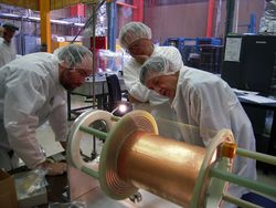
Figure 9 - Prototype stringing and inspection 15
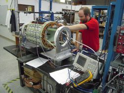
Figure 10 - Prototype assembled and under test 15
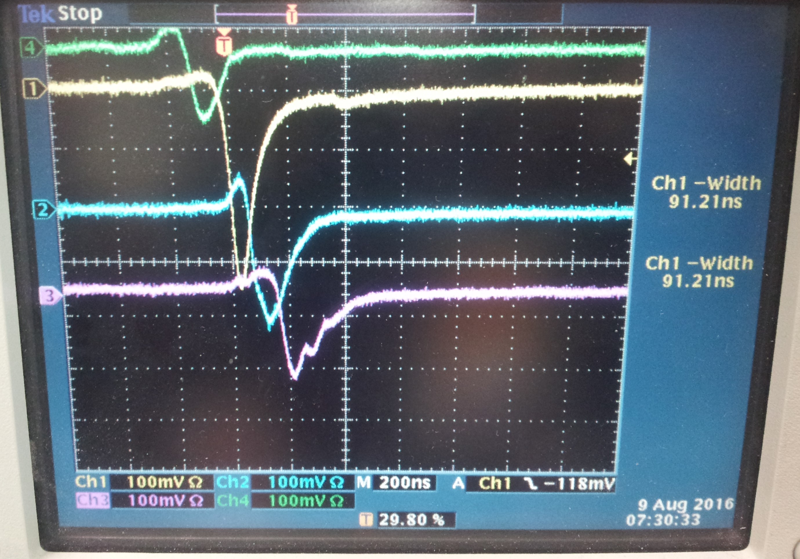
Figure 11 - Cosmic pulse from 4 consecutive channels 15
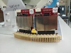
Figure 12 - High Voltage distribution card with Anode pre-amp 15
Figure 13 - High Voltage distribution card placed on chamber 15
Figure 14 - Cathode pads with pad connectors and FR4 ribs structure 15
Figure 15 - Potting shell for the HV capacitors of the Anode Wire Card 15
Figure 16 - Cathode pad adaptor card with pre-amp 16
Figure 17 - HV supply, Network switch and VME crate with Grif-16 + Clock Dist. Module 16
Figure 18 - Cathode pad readout board before assembly 16
Figure 20 - Drift time distribution (maximum drift time 4us) 16
Figure 21 - Track reconstruction (red line) based on drift time 17
Figure 22 - Arrival time distribution and Garfield simulation (red line) 17
Figure 23 - New design of the mounting of the sensor assembly at both end of the bar. 18
Figure 25 - SiPM Gain versus Bias Voltage 19
Figure 26 - Breakdown voltage variation across multiple SiPM units 19
Figure 27 - Air gap versus optical compound puck 19
Figure 28 - DN versus Temperature 20
Figure 29 - Dark count rate versus Temperature 20
Figure 30 - Time resolution setup. Test has been done on 3 SensL devices 21
Figure 31 -Signal sample and CFD timing extraction 21
Figure 32 - Initial time resolution without time versus charge correction. 21
Introduction
This document is to describe the radial TPC gas system for the ALPHA-g Experiment.
The original design of the rTPC has been gone through a major revision in 2014-2015. Optimization and further studies have been done to confirm the feasibility of the use of a radial TPC for the ALPHA-g experiment. The actual design of the radial TPC has been mainly focused during late 2015 with its final design in early 2016.
The rTPC detector itself, as well as its electronics and the data acquisition scheme, are entirely designed in-house by the different groups in the Science Technology Department - Detector group, Detector Electronics group, Electronics group, Data Acquisition group. External manufacturing help (Montreal, SFU, York) are already in place and successfully used.
Purpose
The ALPHA-g experimental goal is to make a first worldwide measurement of the gravity for the antihydrogen atom. This measurement is done in 2 phases
- Up / Down measurement, where the gravity is qualitatively tested and an initial result will demonstrate the sense of the gravity pull on the antihydrogen.
- A quantitative measurement of the gravity pulls with a 1% precision.
Scope
The scope of this project is to manufacture, assemble, test and deliver a detector assembly for the ALPHA-g experiment at CERN. This detector assembly is composed of 2 main parts
- The radial TPC and the Barrel Scintillator
- The Triumf responsibility will include the related firmware and software tools required for its operation and monitoring of the data collected by the detector.
Once the anti-hydrogen (anti-H) is created and maintained in a magnetic “bottle” – Trap –, the annihilation of the anti-H on the wall of the bottle is the sole method to confirm its past presence. The position of the annihilation is what needs to be recorded and the detector will measure the annihilation vertices by tracking the annihilation products (mostly pions) originating from the interaction of the anti-H with matter (trap walls). From the location of the annihilation on the trap wall, the data analysis with further external experimental information will generate the results for the experiment objective. The TPC is to provide the necessary information from all the by-products of the annihilation for track and vertex reconstruction.
Definitions and Abbreviations
General acronyms or terms used for the ALPHA-g experiment
| rTPC | Radial Time Projection Chamber |
|---|---|
| AD | Antiproton Decelerator (CERN building where ALPHA-g is installed) |
| Triumf-ALPHA-g | Refers to the Triumf staff team working on the rTPC detector |
| Trap | Penning trap, magnetic environment preventing the charged particle to escape a defined volume. |
| SSD | Silicon Strip Detector |
Table 1 – ALPHA-g Abbreviations
Detector Concept
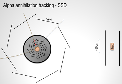
The ALPHA and ALPHA-II experiments track the antihydrogen annihilation using Silicon Strip Detector (SSD). These devices are placed as close as possible to the trap in order to obtain the best position resolution for annihilation vertex measurements.
For the ALPHA-g, the trap is to be longer and make the use of the SSD too expensive.
Alternative solutions have been considered, such as:
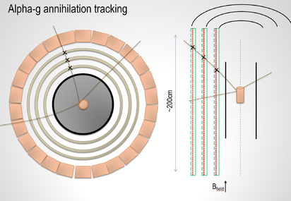
Cylindrical GEMs or Micromegas providing at least 3 intersection points (similar to the SSD configuration but on a larger scale Figure 1). The ASACUSA experiment uses a tracker based on 2 layers of double-sided Micromegas tracker. The detector is used for monitoring of antihydrogen production with high rates. No details have been published on this detector, but their design is based on a tracker for the CLA-12 experiment at J-Lab. This type of the detector will have a limited pattern recognition capability since the cells are connected in one direction on the front-side, and in the other direct in the backside. Also, this detector cannot be made very large without having significant dead region. Furthermore, covering a large area would be expensive (Figure 2).
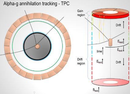
Standard TPC concept is an attractive proposition as this type of detector is well known and Triumf has experience with such device. In this particular case, the geometry is odd as the drift distance is ~2 meter in a restrained space of 7cm. The main reasons for rejecting this option are: 1) we wish to retain the possibility of operating the TPC with low or no axial magnetic field, (2) the non-uniform fringe magnetic fields from the magnetic trap may disrupt the long axial drift of the electrons (by sending them to the walls). Furthermore electron drifting in this volume would be affected by, inhomogeneity of the field cage, large transversal and longitudinal diffusion for such a restricted signal collection region. The latter region is to provide signal gain and such a multiplication cannot be done without using GEMs or MicroMegas devices. Here again, the challenges are multiple in the drift region as well as in the gain region. Channel density is to be very high for proper track information recovery. Figure 3
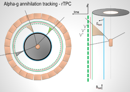
Radial TPC is a compromise as the channel density is reduced by distributing the gain region over the cylinder surface of the detector. Electron multiplication is produced with standard wires stretched between the two ends of the cylinder. In this configuration, the magnetic field (vertical) is perpendicular to the electric field generating a Lorentz force on the traveling electron towards the anode. This results in a spread of charge over several wires from a single particle track crossing the drift volume. B-field homogeneity, E-field non-linearity are to be considered and a particular design note is filed. Figure 4 Figure 3
Figure 1 - Silicon Strip Detectors configuration
Figure 2 - GEMs or Micro-Megas tracking configuration
Figure 3 - Standard TPC configuration
Figure 4 - Proposed Radial TPC configuration
Various simulations studies have been performed to develop and validate the detector concept. The simulation results are presented in the dedicated Detector Simulations.
ALPHA-g Detector Setup
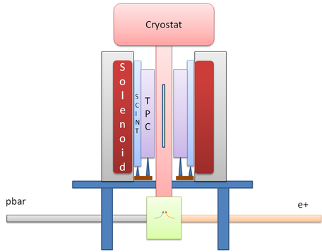
The ALPHA-g experiment setup is composed of
- Antiproton delivery beamline (pbar)
- Positron delivery beamline (e+)
- Cryostat containing the experiments traps
- Radial TPC surrounding the cryostat
- Barrel Scintillator surrounding the rTPC
- Solenoid magnet enclosing the overall detector
Figure 5 - General ALPHA-g experimental setup
The detector part of the experiment is then composed of multiple components from which this report talks only about a subset of them:
- The Radial TPC physical detector and its associated electronics.
- The Barrel Scintillator and its associated electronics.
- The software and acquisition system required for the operation and monitoring of the rTPC and the Barrel Scintillator
- External and Endcap Scintillators (not shown in Figure 5)
The other components – non-discussed in this document – are related to:
- The experiment infrastructure as a whole
- The antiproton, and positron transport lines to the rTPC
- The cryostat and internal Penning traps for the creation of the antihydrogen atoms
- The Hardware and Software involved in the overall trap operations and monitoring
Radial TPC
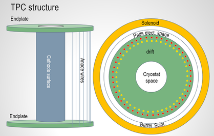
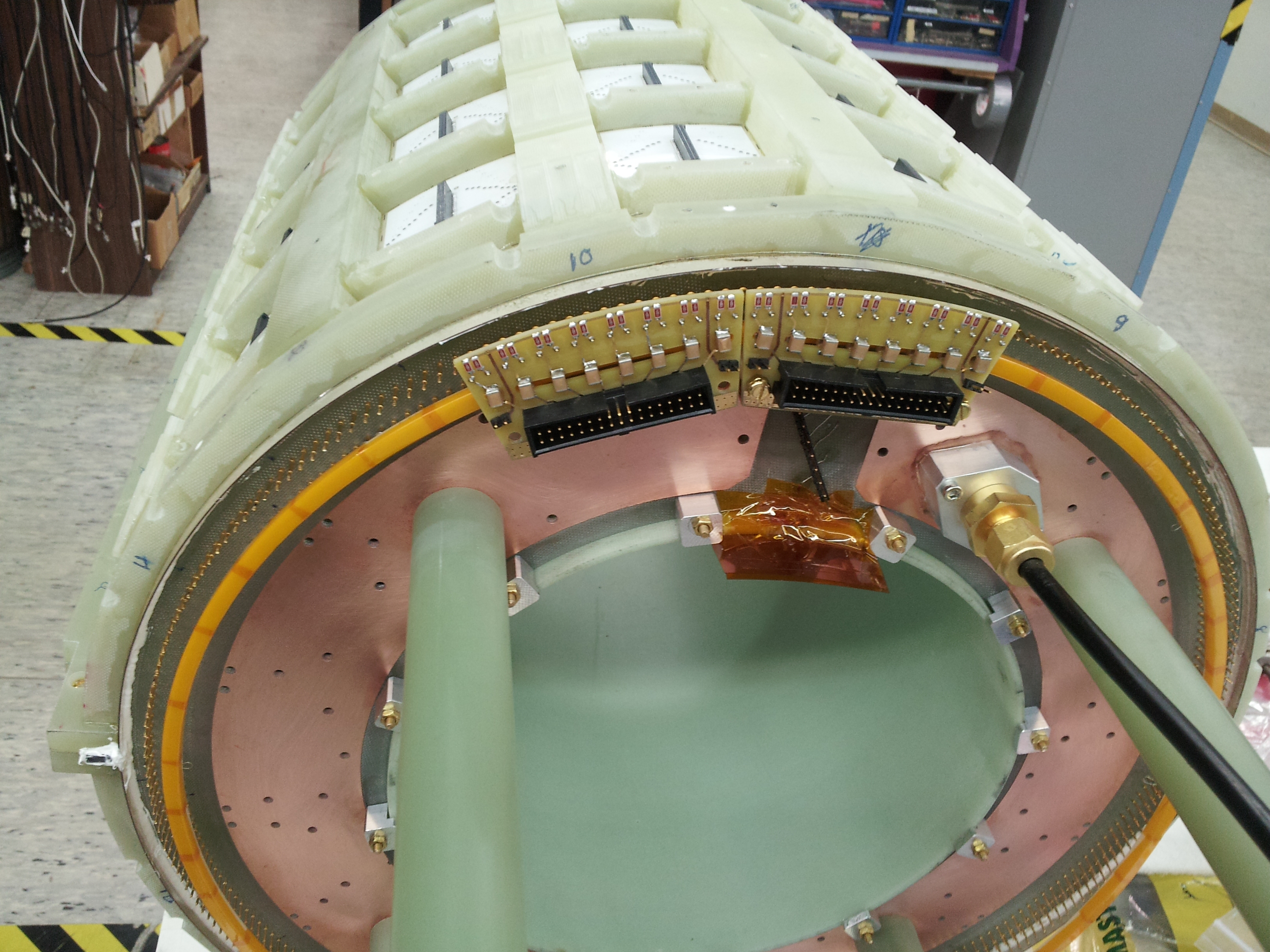
The rTPC is a cylindrical detector composed of an inner cylinder with 2 endplates from where the field and anode wires are strung in between. Part of the electronics is placed on the outer surface of the rTPC and surrounded by the Barrel Scintillator.
Figure 6 - ALPHA-g rTPC and Barrel Scintillator, sketch side and top view
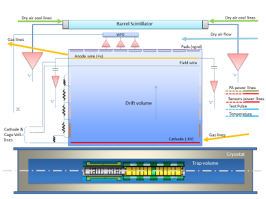
The concept of the rTPC particle detection capabilities requires the registration of the drifted electrons generated by the particle crossing the drift volume. The initial electron is multiplied on the vicinity of the anode wire and an electrical signal is developed on the anode wire. A corresponding induced signal is also visible on the pads placed on the inner surface of the outer cylinder providing another position information (z).
The Detector Simulation Design Notes document is answering the physics operation of the radial TPC.
Figure 7 - Detector concept for the ALPHA-g experiment Bottom shows the ALPHA-g antihydrogen trap within the cryostat. Surrounding the cryostat the rTPC with its electronics components for track recording. At the top the Barrel Scintillator with associated analog electronics.
Prototype Phase
The prototype phase is to construct a section of the overall rTPC length (1/8) with the radial dimensions being not scaled down.
The purpose of this prototype is to confirm several points such as:
Mechanical design & assembly procedure
Gas volume sealing design
High Voltage operation and stability
Frontend electronics operation
The anode wire & pad signal quality
Overall power distribution
DAQ development.
Initial data set for:
Signal comparison to Garfield simulation
Offline simulation data
Signal processing & track reconstruction
Studies of gas mixture
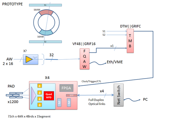
The rTPC prototype is partially equipped with anode wires and cathode pads electronics. Necessary external trigger is provided by (2 scintillator panels) S1.S2 NIM logic and fed to the 2 prototype digitizers boards (GRIF-16). Standard Midas DAQ system is to collect and store the cosmic data.
This prototype setup will remain available for further data acquisition for data analysis, track reconstruction, but also for upgrading the DAQ to its final configuration.
Fabrication and assembly of the final rTPC will be happening in parallel of the continuous prototype tests. We may perform a beam test at M11 to optimize the analysis routine and to best understand the prototype detector.
Figure 8 - Prototype setup. Initial implementation of the Data path is shown. This setup is to remain active for further DAQ and data quality tests.
Notes of December 2016
The fabrication and assembly of the prototype has been completed by mid-August. The associated electronics for anode wire is connected up to 8 100Msps digitizers. The data acquisition has been since then in operation. The cathode pad readout electronics is not yet available.
In summary, the different steps to reach this milestones were:
Gluing of the radial and transversal G10 ribs to the 2 cathode half-cylinder.
While this operation has been successful, the working time with the glue is too short to envisage the gluing of the full length rTPC. New glue candidate has been identified for that job.
Placements and soldering of the cathode pads connectors on the 2 half-cylinder pad boards.
While this operation is possible it is time consuming. New procedure for the soldering and modified jigs have made to simplify this operation.
Field wires and Anode wires stringing. The procedure has worked well and we were able to string the whole chamber (512 wires total) in about 2 weeks.
While single person shift was possible for stinging the prototype, we expect to have 2 persons per shift to complete the stringing of the full chamber in about the same amount of time.
Closure of the chamber, HV and GND connections.
No major issues have been identified, therefore the current design is sound.
Gas leak test
Once all the crimp pins were sealed and holes (mounting holes) blocked, the chamber has been put under gas (Ar/CO2 70/30) and a gas leak less than 5% has been measured.
Installation of the High Voltage distribution cards (AWC) and initial high voltage test.
The AWC provides the 3.2KV to the anode wires. While the HV capacitor were coated with a corona dope to prevent any high voltage breakdown, corona effects have been seen and heard coming from the surface of the HV capacitors. After several unsatisfactory improvements of the isolation of these capacitors, a new design of the card is in progress and full encapsulation of the capacitors in plastic is foreseen. This issue is not affecting the operation of the chamber at short and mid-terms, but need to be resolved for the final detector where humidity and operation condition are less controlled than in the lab.
A potting document has been written which describes the new procedure. It can be found in the Elog entry 217. (https://daq.triumf.ca/elog-alphag/alphag/217)
After appropriate gas flushing, the nominal high voltage have been applied to the chamber while monitoring the individual current (Cathode -4KV, Field: -300V, Anode: +3.2KV). Using 55Fe and cosmic rays, initial evaluation of the anode wire signal have been made using the final anode pre-amp board (AWB).
Readout system acquiring the AWB signals up to 160 channels has been setup and are composed of:
Low voltage distribution for the anode pre-amp boards using the foreseen power cable, but temporary power supplies.
Use of the foreseen signal cable (8m long) from the anode wire board to the WFD in the VME crate.
Prototype DAQ system has been put in place and is composed of:
Full VME crate hosting the available 10 Grif-16 and the Clock distribution module.
Use of the foreseen Griffin WFD board (Grif-16) but using the 100msps instead of the 62.5Msps for now, and the associated clock and trigger distribution modules.
Use of a dedicated network 10Gb switch for local data acquisition.
Grif-16 firmware for ALPHA-g with external trigger capability.
Midas DAQ software for network data acquisition from the 10 Grif-16 boards. Including dedicated UDP frontend and standard data logging.
Online analysis software for individual waveform display.
Offline analysis software for initial track reconstruction based on wire information.
The cathode pad signal acquisition board is not yet available. But interface board to permit the signal evaluation using the anode wire pre-amp has been made. This allowed us to confirm the induced signal on the cathode pads to be about one tenth in amplitude of the anode wire.
Prototype tests
Several High Voltage scans have been made to confirm the nominal voltage operation for the anode at 3.2KV, scan up to 3.6KV. (REF)
Several Gas mixture have been tested such as Ar/CO2: 90-10, 80-20, 70-30, and 60-40. The results confirm the change of the electron drift time as expected by the literature. (REF)
The prototype fabrication highlighted some minor design problems that fortunately were correctable or will be corrected for the full detector. The operation stability of the chamber is acceptable as no HV breakdown have been notified through several weeks of continuous operation.
Presently every channel (anode wire) of the chamber is tested for signal quality. Two “hot wires” have been identified and one of them fixed by “revers-biasing” the chamber. The remaining hot-wire is still under investigation but will not stop the overall checkup procedure of the chamber.
The cathode pad readout board is the next element to be placed on the prototype and we expect to confirm its operation by the end of September. Delays for its realisation are due to the complexity of the PCB layout.
|
Figure 9 - Prototype stringing and inspection |
Figure 10 - Prototype assembled and under test |
|---|---|
|
Figure 11 - Cosmic pulse from 4 consecutive channels |
Figure 12 - High Voltage distribution card with Anode pre-amp |
|
Figure 13 - High Voltage distribution card placed on chamber |
C:\Users\midas\AppData\Local\Microsoft\Windows\INetCache\Content.Word\20160804_121915.jpg Figure 14 - Cathode pads with pad connectors and FR4 ribs structure |
Figure 15 - Potting shell for the HV capacitors of the Anode Wire Card
|
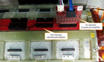
Figure 16 - Cathode pad adaptor card with pre-amp | |
|---|---|
|
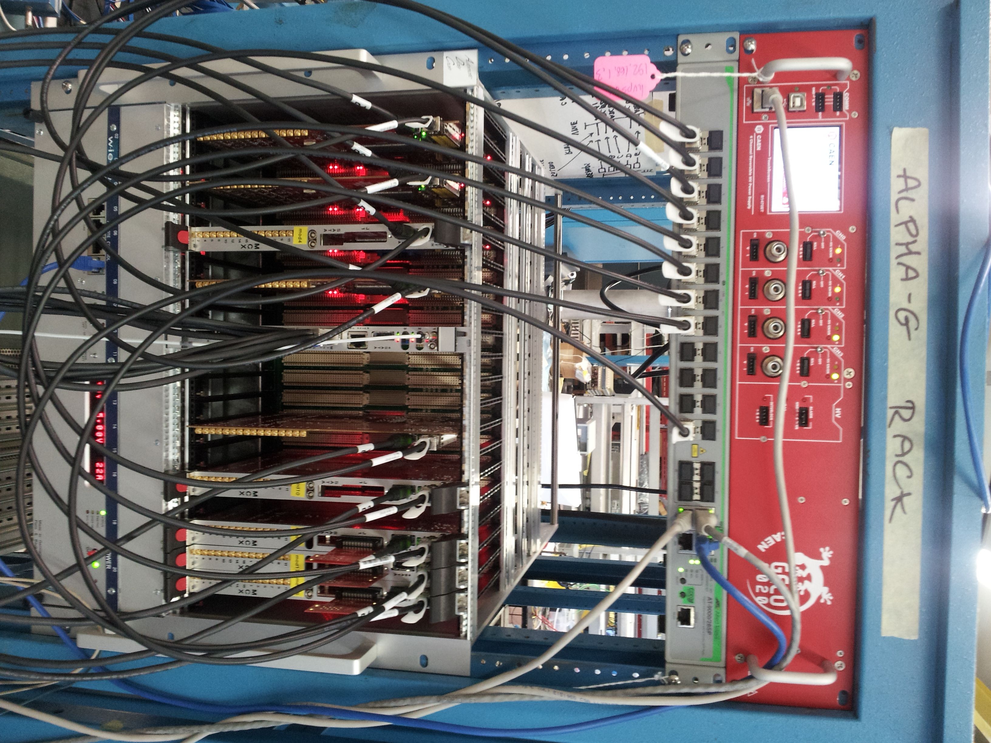
Figure 17 - HV supply, Network switch and VME crate with Grif-16 + Clock Dist. Module |
C:\Users\midas\AppData\Local\Microsoft\Windows\INetCache\Content.Word\20160902_162056.jpg Figure 18 - Cathode pad readout board before assembly |
|
Figure 19 - Section of the chamber under test (external trigger from S1(top Scint.) .S2(bot Scint.) |
Figure 20 - Drift time distribution (maximum drift time 4us) |
|
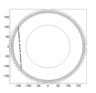
Figure 21 - Track reconstruction (red line) based on drift time |
C:\Users\midas\AppData\Local\Microsoft\Windows\INetCache\Content.Word\roft_run95.png.png Figure 22 - Arrival time distribution and Garfield simulation (red line) |
Data Acquisition
An important fraction of the ALPHA-g project is dedicated to the electronics required for the readout and data collection of the detector. Fortunately, previous development by the “Electronics Development” group can be re-used or used as a starting point for further ALPHA-g requirements. The GRIFFIN data acquisition architecture has similar features that ALPHA-g. Electronics boards are already available and fit our needs. The effort is mostly in the firmware customization, which is largely common to GRIFFIN and ALPHA-g experiment.
One particular new electronics board is the “PadWings” board which handle 288 cathode pads of the rTPC and transmit its data through Gbit optical link. This board uses the ASIC AFTER SCA that we already have experience with for the T2K FGD where close to 300 chips are currently in operation at Tokai.
The overall data acquisition software is left to the Midas package. In particular with the T2K and DEAP and current ALPHA-II experiments, the Midas software has proven its flexibility and versatility. Software effort will be focused on the system integration with the CERN infrastructure in term of data configuration (database), data storage and analysis. Good understanding for this type of specific implementation and issues have already been dealt with for DEAP and ALPHA-II.
Barrel Scintillator
The barrel scintillators surround the rTPC over its full length. A primary purpose is to provide cosmic track detection/rejection via time of flight differences. Preliminary MC studies show that timing resolution of ~300ps will differentiate >90% of cosmic ray events.
The barrel is composed of 64 scintillating bars of trapezoidal shape with a length of 2.6m. Due to the solenoid magnetic field and the restricted space at both end of the detector, the readout is done by multiple SiPM per bar (6). The mechanical integration design and the electronics channel have already been defined. See Figure 26 and Figure 27.
Figure 23 - New design of the mounting of the sensor assembly at both end of the bar.
File:Image25.png File:Image26.png
Figure 24 - 3D-Model of the sensors. Visible the bar in pink, the SiPMs in grey and the signal connections in orange.
The ALPHA-g rTPC project doesn’t include the realization and fabrication of the barrel scintillator prior Q1’ 18. But single bar setup is already in place (DetFac) for signal/timing studies, and will be in use based on the resources availability throughout the year ’16 and ’17. While results from the 2 prototype bars are being collected and analysed, the mechanical design of the Barrel Scint. did restart in December 2016.
SiPM for the Barrel Scintillator studies
Breakdown voltage
The SiPM devices from SensL have the advantage to have a very narrow variation of the breakdown voltage across units. When multiple sensors are needed (such as in our case where 6 will be looking at the same light source), the gain variation between units is negligible and permit to operate group of sensors under the same operating voltage.
Figure 23 shows the gain at different bias voltage for different light intensity. The crossing point at gain zero refers to the breakdown voltage. Repeating the test for each individual sensors (8) gives the overall breakdown voltage of 0.4V. The SensL datasheet indicates a variation of 0.5V.
Figure 25 - SiPM Gain versus Bias Voltage
Figure 26 - Breakdown voltage variation across multiple SiPM units
Sensor interface to the scintillating bar
Mechanically the assembly of the sensors and the barrel Scintillator is delicate as the 64 bars are supported by a support ring (Figure 25, Figure 26). The sensor contact to the bar is to be maintained and reproducible. This interface can be air or an optical compound (puck) see Figure 25. Results shows an increase of light collection over 40%. This puck will also provide a soft cushion which should help in the long term, mechanical issues.
Figure 27 - Air gap versus optical compound puck
Temperature effects
Temperature has a great impact on Silicon based devices. This is the case for the SensL sensor as well. The dark noise is strongly dependent on temperature and we foresee to cool the SiPMs in order to reduce this background noise. With a dedicated setup we recorded the dark noise rate based on temperature, Figure 28. The results in Figure 28 shows a reduction of 2 for 10 °C.
Figure 28 - DN versus Temperature
Figure 29 - Dark count rate versus Temperature
Time resolution
The main goal of the barrel scintillator is to provide time information. Test with final scintillating bar geometry using electron source and SensL units (Figure 30) shows an initial time resolution of the order of 450 ps (Figure 32). One possible contributor of this width is due from the solid angle emission of the Sr-90 on the surface of the bar. Resolution improvement can also be expected by correction of the timing based on the pulse charge in addition to the current CFD algorithm used (Figure 31).
Figure 30 - Time resolution setup. Test has been done on 3 SensL devices
Figure 31 -Signal sample and CFD timing extraction
Figure 32 - Initial time resolution without time versus charge correction.
External and Endcap Scintillators
This system comprise two set of scintillator circumventing the ALPHA-g detector. It serves the following purposes:
External Scintillators
These will consist of scintillator panel pairs external to the magnet, similar to those presently in use in ALPHA2. Their purpose is to provide antiproton counting during initial phase trapping and Hbar production studies. The 2 panels in a pair will be operated in coincidence and as well in coincidences with other pairs.
The design, fabrication and implementation is taken care by the ALPHA-g collaborator of Uni. of York (Scott Menary). The external scintillator is required in late 2017
Endcaps Scintillators
The End caps is to close the “hole” at the top of the detector for catching the comics…
Figure - Veto detector sketches
The Veto endcap detector is to cover the missing coverage of the barrel Scintillator. Initial conceptual design has been put forward, but no final decision has been made on its final implementation.
Specifications
The following table summarize the characteristics of the ALPHA-g detector in term of mechanical, electronics and services.
| Drift | Element | unit | Value |
|---|---|---|---|
| Wire length | mm | 2300.0 | |
| Anode wire diam. | um | 30.0 | |
| Anode wire material | Au/W | ||
| Anode wire tension | g | 40.0 | |
| Field wire diam. | um | 75.0 | |
| Field wire material | Au/Cu/Be | ||
| Field wire tension | g | 120.0 | |
| Cathode pad size | mm | 3.8x37.1 | |
| Cathode pad pitch | mm | 4.0 | |
| # of pad per circumference | 32.0 | ||
| Cathode Voltage | V | -4000.0 | |
| Field Voltage | V | -223.0 | |
| Anode Voltage | V | 3200.0 |
| Gas | Element | unit | Value | Additional info |
|---|---|---|---|---|
| Gas mixture | Ar/CO2 | |||
| Gas mixture range | 90/10 .. 50/50 | |||
| Gas flow | cc/min | 300 | ||
| Gas volume in detector | l | 178.8 | ||
| Flushing time | H | 3.0 | ||
| ip per cm | 90.0 | |||
| Drift length | mm | 64.8 | To the Field wires | |
| E drift | V/cm | -617 | ||
| Electron velocity | cm/u - ns/mm | 1.8 | 57.1 | |
| Diffusion longitudinal | u/cm | ~150 | Ar/CO2 70/30 | |
| Diffusion transversal | u/cm | ~130 | Ar/CO2 70/30 |
| Mechanics | Element | unit | Value | Additional info | |
|---|---|---|---|---|---|
| Inner tube diam. including GND+protection | mm | 211.6 | 105.8 | 0.5mm of Faraday wall | |
| Central Cathode inner tube diam. | mm | 218.4 | 109.2 | on which the cathode foil is glued, add 25um for foil thickness | |
| Field wire position diam. | mm | 348.0 | 174 | ||
| Anode wire position diam. | mm | 364.0 | 182 | ||
| Cathode Pad position diam. | mm | 380.0 | 190 | ||
| TPC active length | mm | 2304.0 | |||
| TPC inner volume length | mm | 2354.0 | |||
| Inner tube length | mm | 2392.6 | 8*228+2*44.3 | ||
| Endplate thickness | mm | 12.5 | |||
| Central cathode wall thickness | mm | 3.06 | |||
| Outer cathode wall thickness | mm | 0.5 | |||
| Laser centre radius | mm | 136.2 | |||
| Barrel Scintillator bar length | mm | 2604.0 | |||
| Barrel Scintillator inner diam. | mm | 446.0 | 223 | ||
| Barrel Scintillator outer diam. | mm | 486.0 | 243 | ||
| Barrel Scintillator geometry | mm | TopL23.9xBotL21.9xH20 | Trapezoidal |
| Calibration | Element | unit | Value | Additional info | |
|---|---|---|---|---|---|
| Number strips | 7.0 | ||||
| Strip length | mm/deg | ||||
| Strip width | mm | 6.0 | |||
| Strip pitch | mm | 380.0 | |||
| First strip (top) position | mm | center | center, +/-380, +/-760, +/-1140 | ||
| Strip phi angle | deg | 360.0 | |||
| Rod distance to central cathode | mm | 27.4 | |||
| Laser beam diameter | um | 400.0 | |||
| Beam offset on rod | um | 200.0 | |||
| Beam tilt | deg | 1.3 | |||
| Aluminum work function | eV - nm | 4.06 | 4.06 – 4.26 | 305.4 | |
| Silver work function | eV - nm | 4.27 | 4.26 – 4.74 | 291 | |
| Copper work function | eV - nm | 4.53 | 4.53 – 5.10 | 273.7 | |
| T2K results Al | pe/mm2 | 2.0 | Ratio: 66.66666667 | ||
| T2K results Cu | pe/mm2 | 0.030 |
| Channels | Element | unit | Value | Additional info | |
|---|---|---|---|---|---|
| Numbers of Anode wires | - | 256.0 | |||
| Number of Field wires | - | 256.0 | |||
| Number of rTPC sections | - | 8.0 | |||
| Number of Pads per AFTER chip | - | 72.0 | |||
| Number of AFTER per PadWing card | - | 4.0 | |||
| Number of PadWing card per rTPC section | - | 8.0 | |||
| Number of Pads per rTPC section | 2304.0 | ||||
| Number of Scint. bars | - | 64.0 | |||
| Number of SiPM per Scint. bar | - | 6.0 | |||
| Total number of SiPM sensors | - | 768.0 | |||
| Total number of Cathode Pads | - | 18432.0 |
| Electronics | Element | unit | Value | Additional info | |
|---|---|---|---|---|---|
| Number of Anode Wire Boards AWB | - | 32.0 | Top(16) + Bot(16) | ||
| Number of Anode Card AWC | - | 32.0 | Top(16) + Bot(16) | ||
| Number of channels per AWB | - | 16.0 | |||
| AWB power consumption | A | 0.3 | @ +5V | ||
| AWB power consumption | A | 0.3 | @ -5V | ||
| Total number of PadWings boards | - | 64.0 | |||
| PWB power consumption | A | 1.5 | @ +5.0V | ||
| PWB power consumption | A | 1.0 | @ + 3.0V | ||
| Total number of Anode wire boards | - | 32.0 | |||
| Total number of SiPM board | - | 32.0 | |||
| Anode Wire WaveForm Sampling Freq. | Msps | 100.0 | |||
| Number of Barrel Scint. boards BSB | - | 32.0 | Top(16)+Bot(16) | ||
| Barrel Scint. Waveform Sampling Freq. | Msps | 100.0 | |||
| Grif-16 resolution | bits | 14.0 | |||
| Grif-16 input range | Vpk-to-pk | 2.0 | |||
| Grif-16 sampling rate | Msps | 100.0 | |||
| Grif-16 FMC resolution | bits | 14.0 | |||
| Grif-16 FMC input range | Vpk-to-pk | 2.0 | |||
| Grif-16 FMC sampling rate | Msps | 62.5 | |||
| Rack 43Ux600mmx800mm | 1U=1.75" or 44.45mm |
Table 2 – Detector specification parameters list
